Image sensor and image-capturing device

Active Publication Date: 2018-10-04
NIKON CORP
View PDF4 Cites 0 Cited by
  • Summary
  • Abstract
  • Description
  • Claims
  • Application Information

AI Technical Summary

Benefits of technology

The patent describes an image sensor that improves sensitivity by increasing the number of pixels and maintaining a large light receiving area. The image sensor includes an accumulation unit and a readout unit that accumulate and read out electric charges generated by a photoelectric conversion unit. The accumulation unit and readout unit are positioned along the optical axis direction of a microlens. The image sensor can be used in an image-capturing device to generate high-quality image data.

Problems solved by technology

As the light receiving area is reduced, the amount of electric charge generated by photoelectric conversion decreases, which can lead to a deterioration in the sensitivity.

Method used


Image

  • Image sensor and image-capturing device
  • Image sensor and image-capturing device
  • Image sensor and image-capturing device

Examples


first embodiment

[0024]Schematic Element Configuration

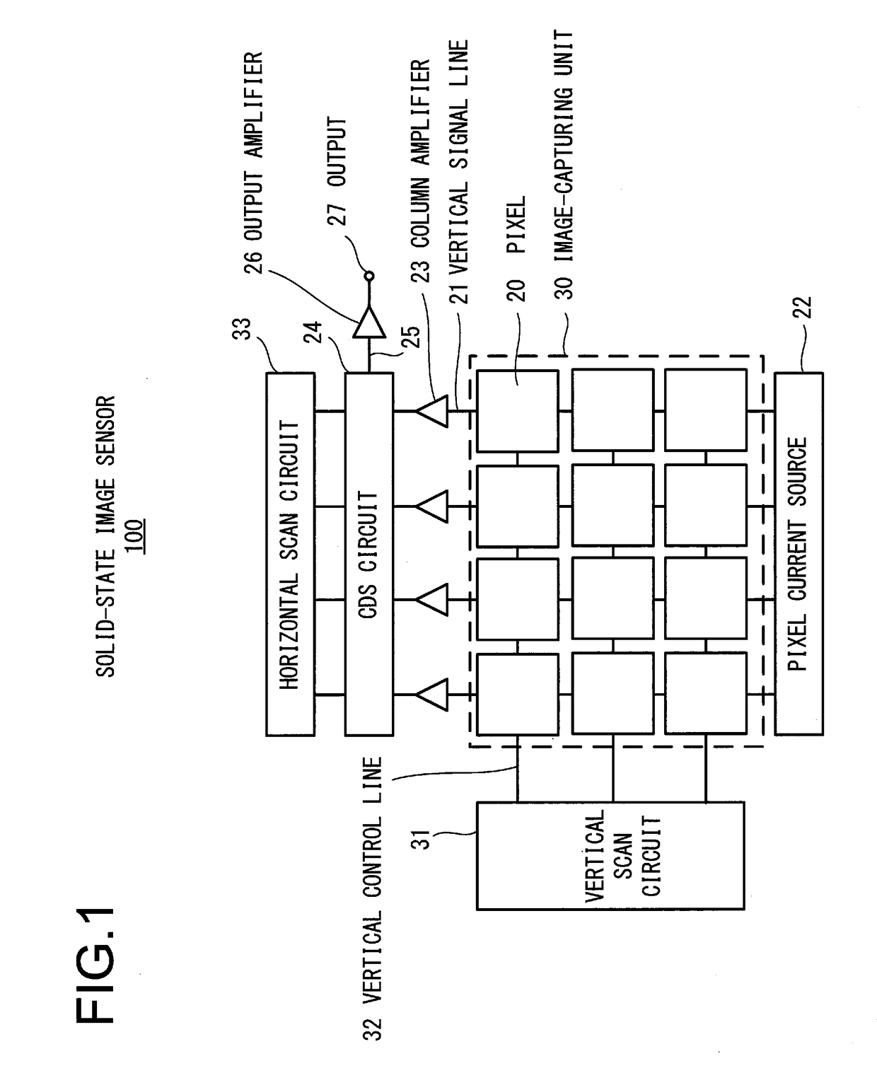
[0025]FIG. 1 is a view illustrating a schematic configuration of a solid-state image sensor 100 according to a first embodiment.

[0026]The solid-state image sensor 100 includes an image-capturing unit 30 having pixels 20 arranged on a light receiving surface. The pixels 20 are supplied with drive signals from a vertical scan circuit 31 via vertical control lines 32. Further, the pixels 20 are connected to vertical signal lines 21 on a column basis. The vertical signal lines 21 are connected to a pixel current source 22.

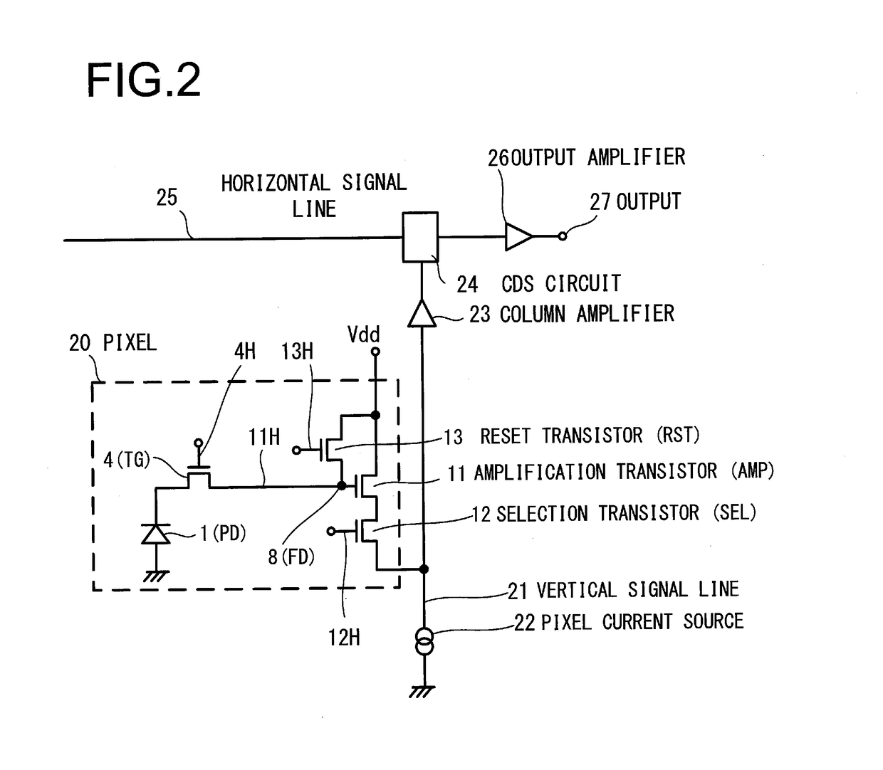
[0027]Furthermore, noise outputs and signal outputs that are time-divisionally outputted from the pixels 20 to the vertical signal lines 21 are sequentially inputted to a CDS circuit (a correlated double sampling circuit) 24 via column amplifiers 23. The CDS circuit 24 calculates a difference between both outputs to generate a true signal output. This true signal output is horizontally scanned by a drive signal from a horizontal sca...

second embodiment

[0151]FIG. 11 is a view illustrating a solid-state image sensor 100A according to a second embodiment. The same parts as those of the solid-state image sensor 100 according to the first embodiment are denoted by the same reference signs, and a detailed description thereof is omitted.

[0152]A semiconductor substrate 202 of the solid-state image sensor 100A has a light receiving surface on a substrate back surface side. The semiconductor substrate 202 includes a flat plate-like base region 202K having a plane extending in the same direction of that of the light receiving surface and a protruding region 202TA having a protruding shape from the base region 202K toward the light receiving surface side.

[0153]The protruding region 202TA has a prismatic shape having a rectangular cross section, and the PD 1 is provided at the uppermost part on the substrate back surface side. The configuration of the PD 1 is the same as that in the first embodiment, and a description thereof will be omitted....


PUM


Abstract

An image sensor includes: an accumulation unit that accumulates an electric charge generated by a photoelectric conversion unit that photoelectrically converts incident light transmitted through a microlens; and a readout unit that reads out a signal based on a voltage of the accumulation unit, wherein the accumulation unit and the readout unit are included along an optical axis direction of the microlens.

Description

TECHNICAL FIELD[0001]The present invention relates to an image sensor and an image-capturing device.BACKGROUND ART[0002]PTL1 discloses the following solid-state image sensor. A semiconductor substrate is provided with an image-capturing region including a photoelectric conversion unit and a signal scan circuit unit and having unit pixels arranged in a matrix. The image-capturing region includes an field isolation insulating film that is provided to correspond to a boundary part between adjacent unit pixels and surround each unit pixel; a MOSFET provided on a front surface of the semiconductor substrate and in a region below the field isolation insulating film; and a first diffusion layer having a first conductivity type provided in a region in the vicinity of the field isolation insulating film in the semiconductor substrate. The field isolation insulating film is provided in the semiconductor substrate at an offset from the front surface of the semiconductor substrate on which the ...

Claims


Application Information

Patent Timeline
IPC IPC(8): H04N5/378H01L27/146
CPCH04N5/378H01L27/14627H01L27/14623H01L27/088H01L21/823487H01L27/14612H01L27/14629H01L27/14634H01L27/14643H01L27/14689H01L27/1469H01L27/06H01L21/8234H04N25/70H01L31/10H01L27/14609H04N25/75
Inventor SARUWATARI, OSAMU
Owner NIKON CORP
Why Eureka
Try Eureka