
Optical imaging device

a technology of optical imaging and optical aberration, which is applied in the field of optical imaging devices, can solve the problems of remarkably occurring distortion aberration and obtained blue and distorted images, and achieve the effects of reducing the number of lenses

Active Publication Date: 2017-07-27
ELECTRONICS & TELECOMM RES INST
View PDF2 Cites 0 Cited by
  • Summary
  • Abstract
  • Description
  • Claims
  • Application Information

AI Technical Summary

Benefits of technology

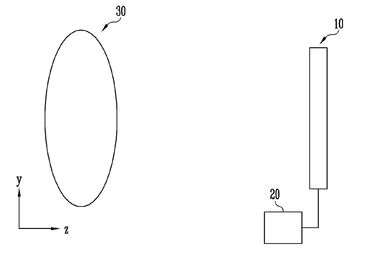
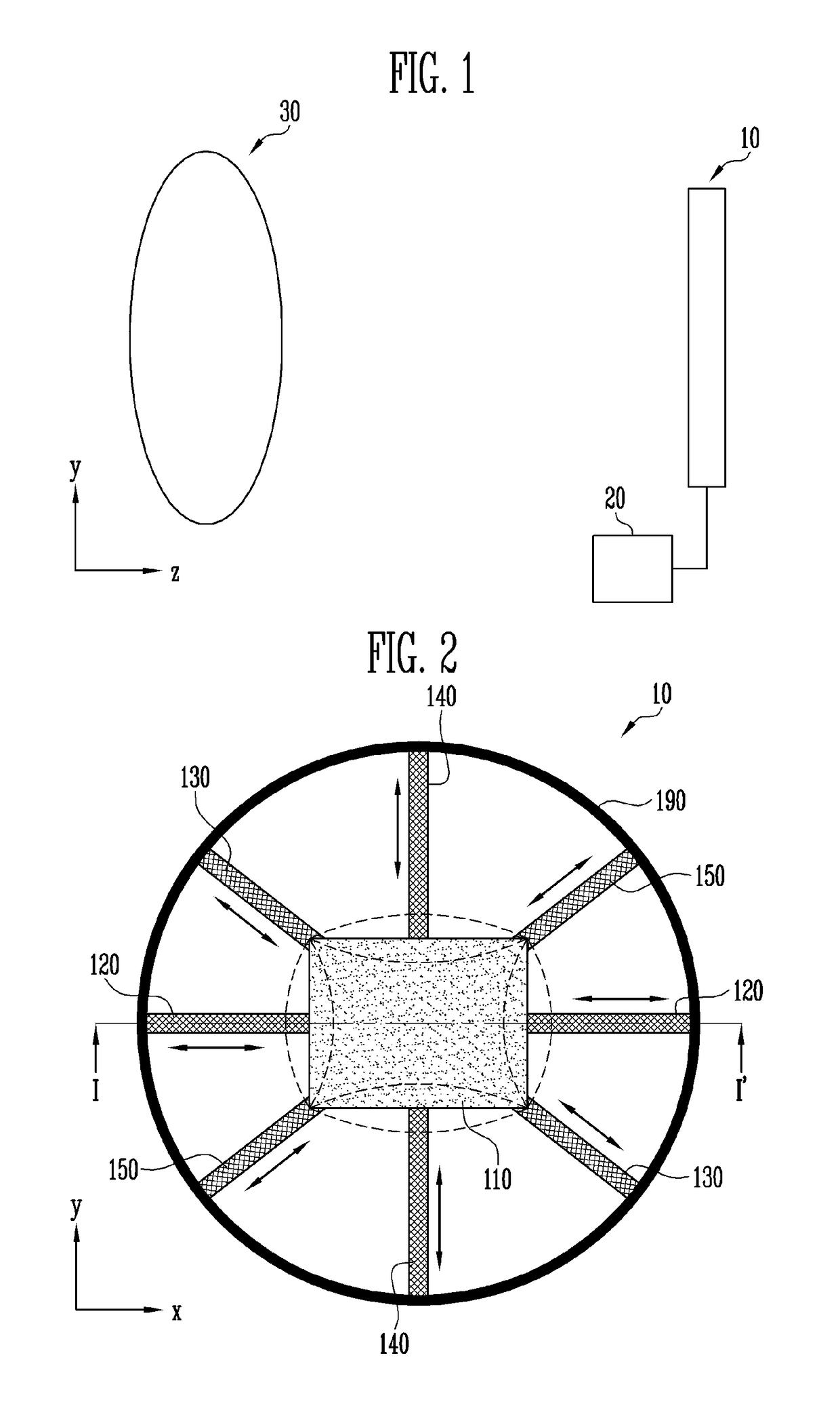
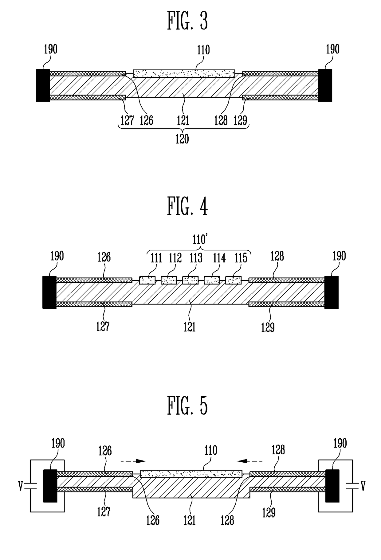
The present invention is about an optical imaging device that can minimize distortion aberration and control the view angle and magnification. The device can expand or contract the image and adjust the viewing angle without moving the lens. By correcting distortion aberration, the device can obtain high-resolution images. Additionally, the device can have a zoom function and control the view angle without moving the lens. This makes it possible to design a small optical imaging device.

Problems solved by technology

However, light that forms an angle with the optical axis of the lens, that is, that is incident in an off-axis manner is focused in front of or behind the image sensor without being correctly focused on the image sensor due to the aberration.
Therefore, a clear image may be obtained in the center of the image sensor, but a blurred and distorted image is obtained at the edge of the image sensor due to the aberration.
When an object such as wire mesh is photographed in parallel with the image sensor surface, the distortion aberration remarkably occurs.

Method used


Image

  • Optical imaging device
  • Optical imaging device
  • Optical imaging device

Examples


Embodiment Construction

[0039]Advantages and features of the present invention, and implementation methods thereof will be clarified through following embodiments described with reference to the accompanying drawings. The present invention may, however, be embodied in different forms and should not be construed as limited to the embodiments set forth herein. Throughout this specification and the claims that follow, when it is described that an element is “connected” to another element, the element may be “directly connected” to the other element or “electrically connected” to the other element through a third element. In the accompanying drawings, a portion irrelevant to description of the present invention will be omitted for clarity. Like reference numerals refer to like elements throughout.

[0040]The scope of the present invention may be applied to any device including an optical device such as a camera and a microscope. Hereinafter, embodiments will be described in detail so that those skilled in the ar...


PUM


Abstract

There is provided an optical imaging device including a flexible image sensor and an actuator that expands or contracts the flexible image sensor on a two-dimensional plane. It is possible to minimize distortion aberration and control a viewing angle and magnification.

Description

CROSS-REFERENCE TO RELATED APPLICATION[0001]This application claims priority to and the benefit of Korean Patent Application No. 10-2016-0009296, filed on Jan. 26, 2016, in the Korean Intellectual Property Office, the entire contents of which are incorporated herein by reference in their entirety.BACKGROUND[0002]1. Field[0003]An embodiment of the present invention relates to an optical imaging device, and more particularly, to an optical imaging device including a flexible image sensor.[0004]2. Description of the Related Art[0005]A camera capable of storing an image as digital information is being continuously developed. A photographing system of the camera includes an image sensor capable of storing optical intensity information. The image sensor may be, for example, a charge coupled device (CCD) or a complementary metal-oxide-semiconductor (CMOS) device. On the other hand, the image sensor may be formed of a plurality of optical sensor arrays. Studies on the camera including the i...

Claims


Application Information

Patent Timeline
Patent Type & Authority Applications(United States)
IPC IPC(8): H04N5/232H04N5/357H04N5/225
CPCH04N5/23296H04N5/3572H04N5/2254H04N5/2253H04N23/54H04N23/50H04N23/69H04N25/61
Inventor PARK, SUN TAKKYUNG, KI UKNAM, SAE KWANGPARK, BONG JEPARK, SEUNG KOOYUN, SUNG RYUL
Owner ELECTRONICS & TELECOMM RES INST
Learn More