
Soldering Device Minimizing Voids When Soldering Printed Circuit Boards

a soldering device and printed circuit board technology, applied in the direction of solventing apparatus, manufacturing tools, heating appliances, etc., can solve the problems of inadmissible field failure, inability to solder the soldering point and/or the components, and the inclusions are habitually formed in the solder between the components and the printed circuit board, so as to minimize the formation of voids and reduce the disadvantages

Inactive Publication Date: 2017-03-16
ERSA GMBH
View PDF11 Cites 0 Cited by
  • Summary
  • Abstract
  • Description
  • Claims
  • Application Information

AI Technical Summary

Benefits of technology

[0008]Proceeding from this state of the art, it is consequently the object of the present invention to diminish the aforodescribed disadvantages and to minimize the formation of voids in the soldering points.

Problems solved by technology

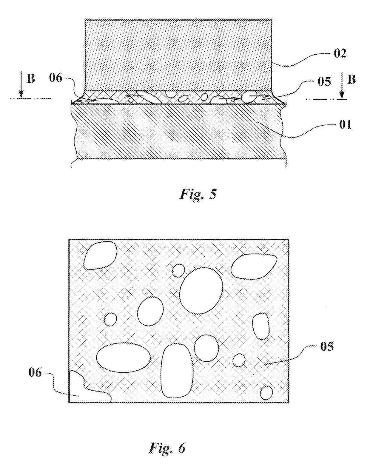
In these known soldering methods, it is disadvantageous that inclusions are habitually formed in the solder between the component and the printed circuit board.
Depending on how many occurrences of voids there are and on the dimensions and the position the same have, said voids can lead to failure of the soldering point and / or the components, which may lead to inadmissible field failures, especially in the area of power electronics and in high-end industries like the aerospace industry.
When soldering under negative pressure, there is, however, in particular the risk that inclusions of water in the molecular chains or in microclearances of the plastic housings of the components and of the printed circuit board substrate, said microclearances being situated between the molecular chains, pass into the vapor phase and try to escape.
This may lead to the plastic housings of the components being destroyed and to the printed circuit boards being delaminated.
When soldering under excess pressure, the voids are not removed; rather they are only compressed and reduced in size, so that, in future alternating temperature loads of the soldering connections, said connections are subjected to a high mechanical load, which may lead to the soldering connections being destroyed.
In this respect, it is in particular disadvantageous that this may lead to an undesirable dislocation in small and midget components and that, without an additional vacuum, the gas inclusions are insufficiently removed.

Method used


Image

  • Soldering Device Minimizing Voids When Soldering Printed Circuit Boards
  • Soldering Device Minimizing Voids When Soldering Printed Circuit Boards
  • Soldering Device Minimizing Voids When Soldering Printed Circuit Boards

Examples


Embodiment Construction

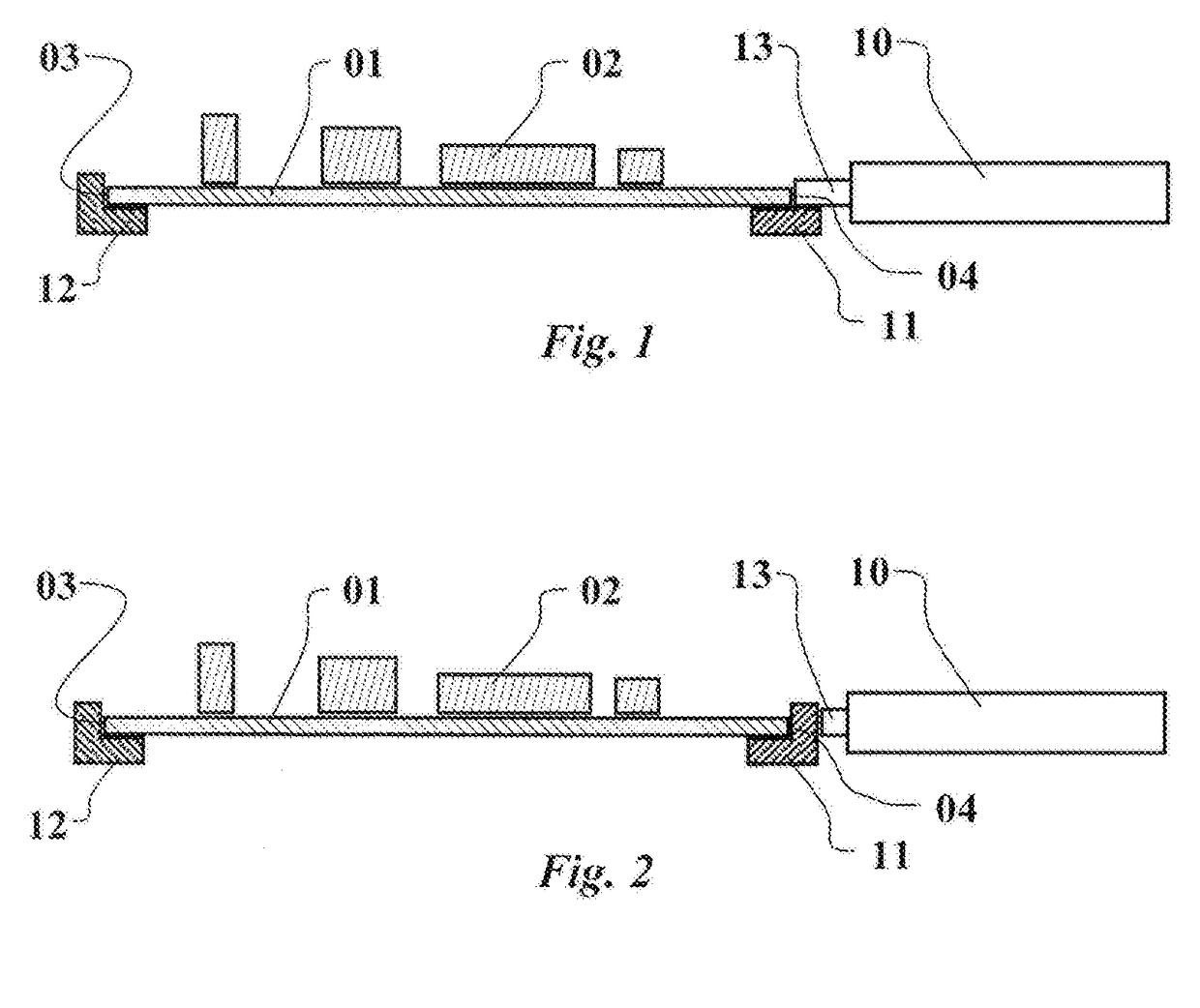
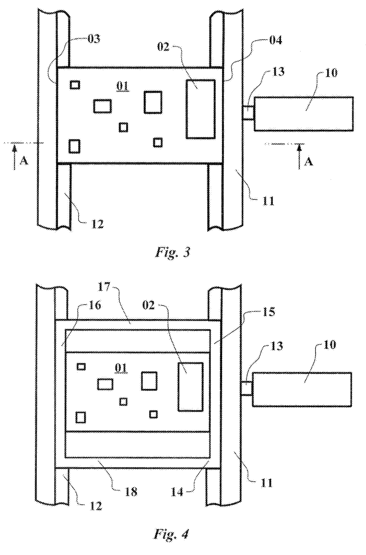
[0039]In FIG. 1, in a first exemplary embodiment, the arrangement of an oscillation generator or actuator 10 for exciting oscillations in as printed circuit board 01 is schematically illustrated. For reasons of a simpler and clearer illustration, the soldering installation in which the arrangement of the printed circuit board and of the actuator is arranged is not illustrated.

[0040]The printed circuit board 01 being equipped with electronic components 02 rests on a pair of carriers 11 and 12. In this respect, the carrier 12 is embodied as an angle that is L-shaped in cross-section, against the vertical leg of which a longitudinal edge 03 of the printed circuit board comes to rest. The carrier 12 is substantially rigidly fixed to a machine rack or to a housing of the soldering installation in a manner that is not illustrated and in this way forms a dead stop for the printed circuit board 01. The carrier 11 that is opposite to the carrier 12 only forms a rest for the lateral edge 04 o...


PUM

PropertyMeasurementUnit
frequencyaaaaaaaaaa
frequencyaaaaaaaaaa
frequencyaaaaaaaaaa

Abstract

A soldering device for soldering a printed circuit board includes at least one heating appliance melting solder situated between electrical or electronic components being soldered onto a printed circuit board and the printed circuit board. At least one actuator mechanically oscillates the printed circuit board at a variable frequency of oscillation in a direction of a plane defioned by the printed circuit board. A second lateral edge of the printed circuit board, the second lateral edge being opposite to the first lateral edge of the printed circuit board, rests against iand supported by a fixed stop.

Description

CROSS REFERENCE TO RELATED APPLICATION[0001]This application is a divisional application of U.S. patent application Ser. No. 14 / 531,860 filed on Nov. 3, 2014 which claims the priority benefit of German Patent Application No. 10 2013 112 367.8 filed on Nov. 11, 2013 and European Patent Application No. 14 186 548.5 filed on Sep. 26, 2014, all of which are fully incorporated herein by reference.STATEMENT REGARDING FEDERALLY SPONSORED RESEARCH OR DEVELOPMENT[0002]Not applicable.FIELD OF THE INVENTION[0003]The invention relates to a method for minimizing voids when soldering printed circuit boards.BACKGROUND OF THE INVENTION[0004]Various methods as well as soldering devices for soldering printed circuit boards being equipped with electrical and / or electronic components are known from the state of the art, wherein a solid-state solder is arranged between the printed circuit board and the relevant component, in particular in the case of components being arranged on the surface area of the ...

Claims


Application Information

Patent Timeline
Patent Type & Authority Applications(United States)
IPC IPC(8): B23K1/00H05K3/34B23K1/008B23K1/06B23K3/04B23K3/08
CPCB23K1/0016B23K3/04B23K3/08H05K2203/1509B23K1/06H05K3/341H05K2203/0292B23K1/008H05K3/3494H05K2203/0285H05K3/303H05K13/0465
Inventor RAWINSKI, VIKTORIA
Owner ERSA GMBH
Learn More