Storage Facility for Semiconductor Containers
- Summary
- Abstract
- Description
- Claims
- Application Information
AI Technical Summary
Benefits of technology
Problems solved by technology
Method used
Image

Examples
Embodiment Construction
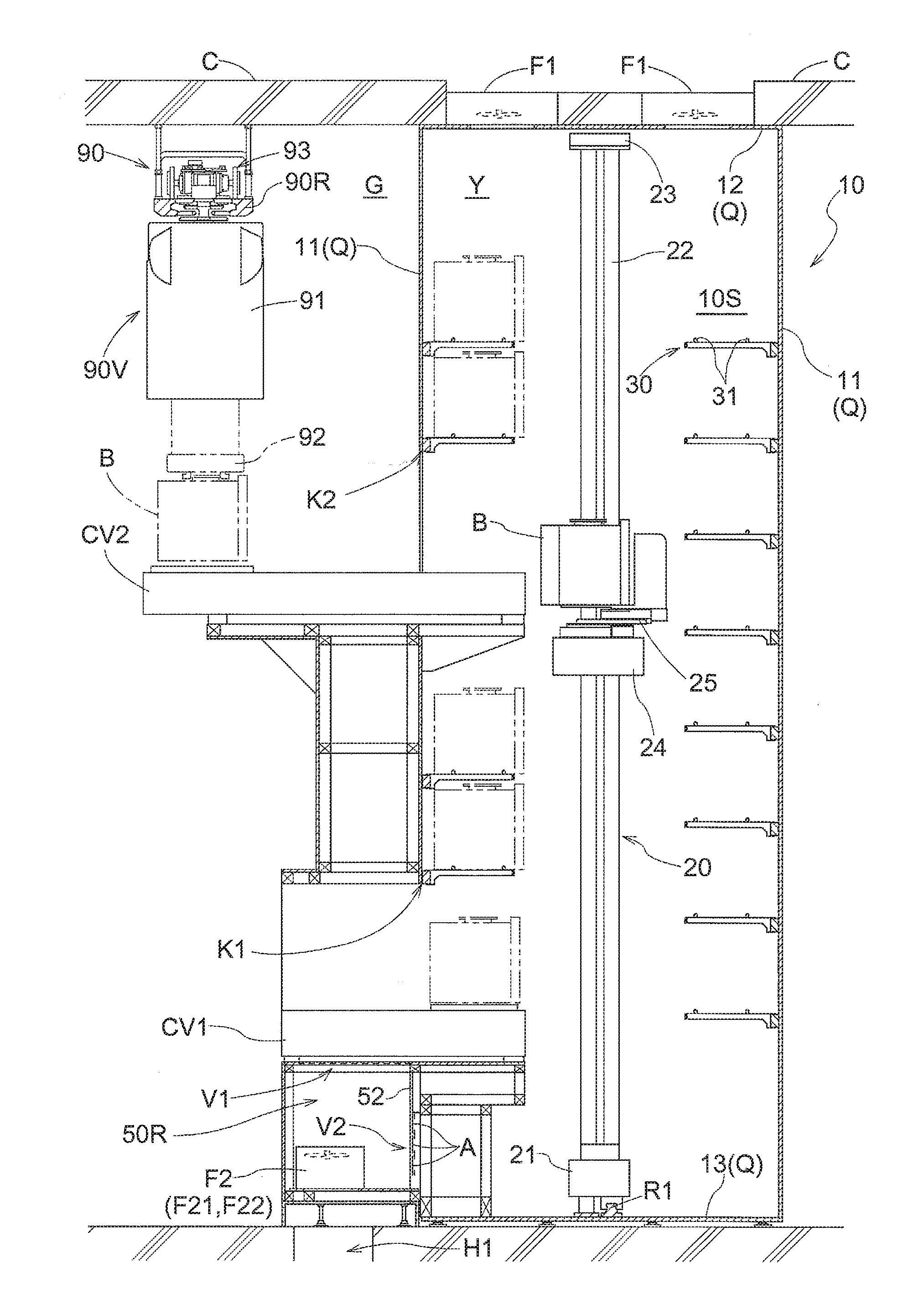
[0019]Embodiments of a storage facility for semiconductor containers are described next with reference to the drawings.
[0020]As shown in FIG. 1, the storage facility for semiconductor containers of the present embodiment includes a storage structure 10 for storing a plurality of containers B (FOUPs) for holding or carrying semiconductor substrates, such that the containers B are arranged one above another in a vertical direction.
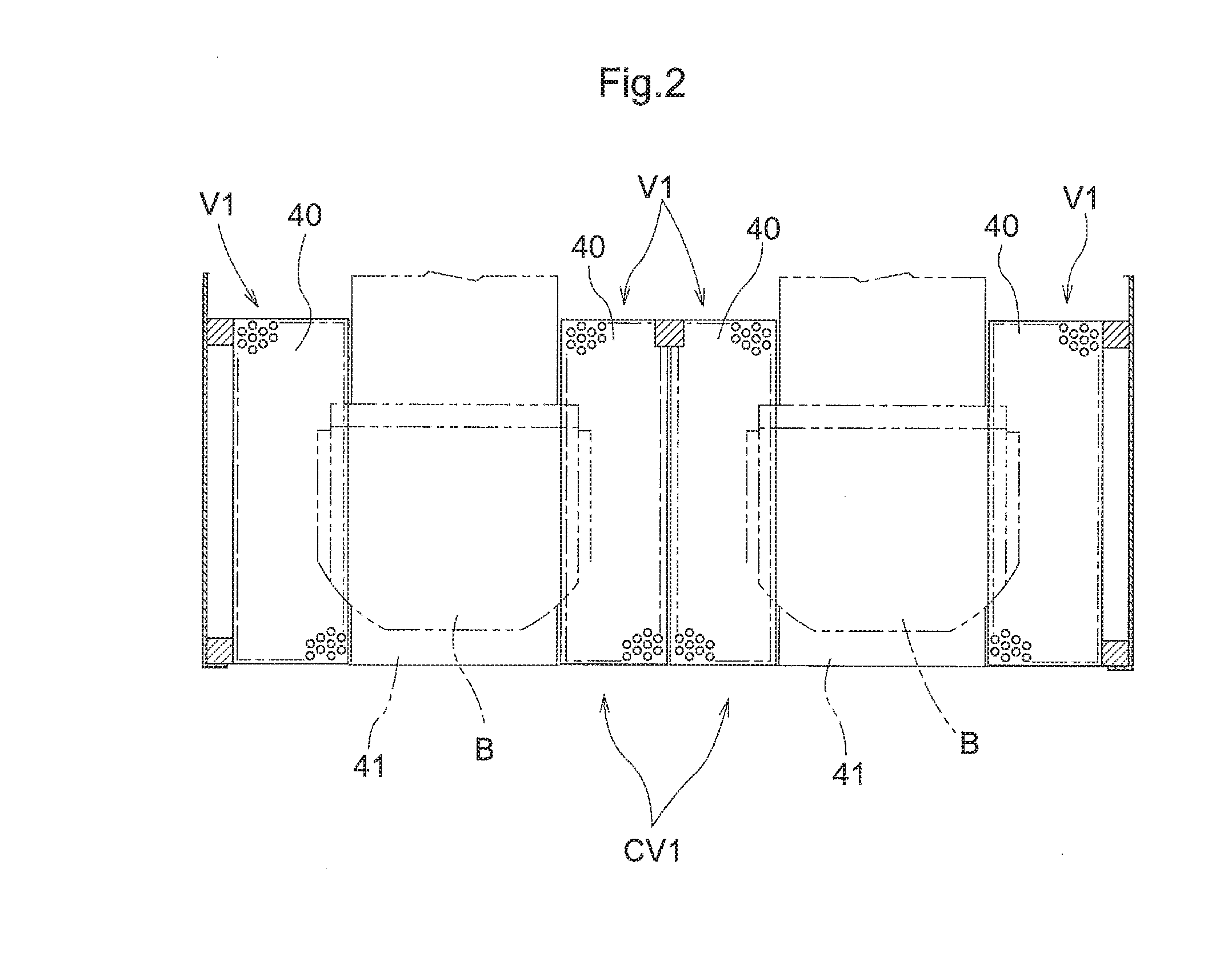
[0021]The storage structure 10 includes partitioning walls Q, and holding space Y, and an inactive gas enriching air supply portion. The partitioning walls Q include side wall portions 11 extending along the vertical direction, an upper base portion12, and a lower base portion 13. The holding space Y is partitioned off from the exterior space G by the partitioning walls Q as seen along the vertical direction. An inactive gas enriching air supply portion supplies inactive gas enriched air, which contains higher concentration of inactive gas (nitrogen etc.) th...
PUM
 Abstract
Description
Claims
Application Information
 - R&D
- Intellectual Property
- Life Sciences
- Materials
- Tech Scout
- Unparalleled Data Quality
- Higher Quality Content
- 60% Fewer Hallucinations
Browse by: Latest US Patents, China's latest patents, Technical Efficacy Thesaurus, Application Domain, Technology Topic, Popular Technical Reports.
© 2025 PatSnap. All rights reserved.Legal|Privacy policy|Modern Slavery Act Transparency Statement|Sitemap|About US| Contact US: help@patsnap.com