Liquid crystal panel and method for manufacturing the same

a technology of liquid crystal panels and liquid crystals, applied in the manufacture of electrode systems, electric discharge tubes/lamps, instruments, etc., can solve the problems of more time, increased manufacturing costs, and dramatic decrease of aperture ratios, so as to reduce manufacturing costs, improve production efficiency, and simplify manufacturing processes

Inactive Publication Date: 2015-07-09
TCL CHINA STAR OPTOELECTRONICS TECH CO LTD
View PDF6 Cites 4 Cited by
  • Summary
  • Abstract
  • Description
  • Claims
  • Application Information

AI Technical Summary

Benefits of technology

[0009]An objective of the present invention is to provide a liquid crystal panel and method for manufacturing the same capable of simplifying the manufacturing process, increasing the production efficiency, and reducing the manufacturing cost, solving the technical problems including complicated processes, low production efficiency, and high manufacturing cost caused in conventional liquid crystal panels.
[0023]Compared to a conventional liquid crystal panel, the liquid crystal panel and method of manufacturing the same in the present invention is quite simple, the production efficiency is improved, and the manufacturing cost is reduced. Therefore, the present invention can solve the technical problems including complicated processes, low production efficiency, and high manufacturing cost caused in conventional liquid crystal panels.

Problems solved by technology

If the liquid crystal panel is relatively small in size, increasing the size of BM may result in dramatic decrease of an aperture ratio.
However, using the afore-described approach to manufacturing the first black matrix 122 and the second black matrix 124 takes more time and the manufacturing cost is relatively high.
To a certain extent, this will reduce the production efficiency of the liquid crystal panel and increase the manufacturing cost.

Method used


Image

  • Liquid crystal panel and method for manufacturing the same
  • Liquid crystal panel and method for manufacturing the same
  • Liquid crystal panel and method for manufacturing the same

Examples


Embodiment Construction

[0034]The following descriptions for the respective embodiments are specific embodiments capable of being implemented for illustrations of the present invention with referring to appended figures. In the descriptions of the present invention, spatially relative terms, such as “upper”, “lower”, “front”, “back”, “left”, “right”, “inner”, “outer”, “lateral”, and the like, may be used herein for ease of description as illustrated in the figures. Therefore, it will be understood that the spatially relative terms are intended to illustrate for understanding the present invention, but not to limit the present invention.

[0035]In the appending drawings, units having similar structures are labeled by the same reference numbers.

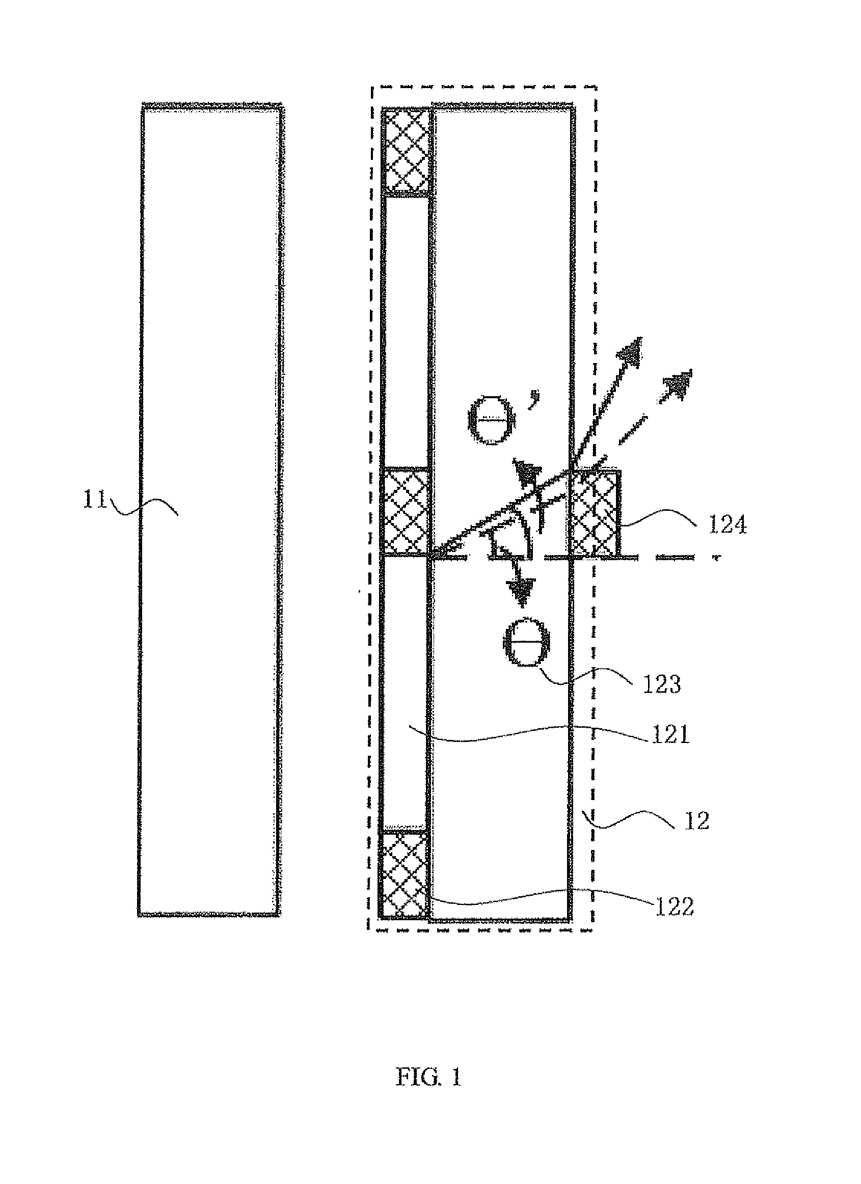
[0036]Please refer to FIG. 2 and FIG. 3. FIG. 2 is a flow chart of a method for manufacturing a liquid crystal panel according to a first preferable embodiment of the present invention. FIG. 3 is a schematic structural diagram showing the liquid crystal panel manufactur...


PUM

PropertyMeasurementUnit
structureaaaaaaaaaa
distanceaaaaaaaaaa
sizeaaaaaaaaaa

Abstract

The present invention relates to a liquid crystal panel and method for manufacturing the same. The liquid crystal panel manufacturing method comprises steps of: manufacturing an array substrate and a color filter substrate, sealing the array substrate and the color filter substrate together, and injecting liquid crystal material therebetween so as to form a liquid crystal cell, the color filter substrate having a first black matrix and a color resistor layer at an inner side thereof; and forming a second black matrix on an external surface of the color filter substrate by ink-jet printing. The liquid crystal panel and method for manufacturing the same is quite simple, the production efficiency is improved, and the manufacturing cost is reduced.

Description

BACKGROUND OF THE INVENTION[0001]1. Field of the Invention[0002]The present invention relates to a liquid crystal display technology, and more particularly, to a liquid crystal panel and method for manufacturing the same.[0003]2. Description of Prior Art[0004]Nowadays, liquid crystal displays (LCDs) have been widely used in displaying 3D images. For example, a 3D liquid crystal display equipped with a film-type patterned retarder (FPR) is developed. In the 3D liquid crystal panel, 3D viewing angle is an important indication, which represents a range of angles a viewer at a certain distance is able to see the 3D images.[0005]The 3D viewing angle can be improved by increasing the size of a black matrix (BM) in a color filter substrate of the liquid crystal panel. However, this approach is merely suitable for large-scale liquid crystal panels. If the liquid crystal panel is relatively small in size, increasing the size of BM may result in dramatic decrease of an aperture ratio.[0006]In...

Claims


Application Information

Patent Timeline
Patent Type & Authority Applications(United States)
IPC IPC(8): G02F1/1335G02B27/26G02F1/1341G02F1/13363G02F1/1339G02B30/25
CPCG02F1/133512G02F1/133516G02F1/133528G02F2001/133354G02F1/1339G02F1/1341G02B27/26G02F1/13363G02F1/1333G02F1/133514G02F2202/28G02F1/133565G02F1/133562G02B30/25G02F1/133354
Inventor YANG, ZANHSIAO, CHIA-CHIANGCHEN, CHIH-WEN
Owner TCL CHINA STAR OPTOELECTRONICS TECH CO LTD
Why Eureka
Try Eureka