
Optical waveguide, method for producing optical waveguide, optical waveguide module, method for producing optical waveguide module, and electronic apparatus

Inactive Publication Date: 2013-07-11
SUMITOMO BAKELITE CO LTD
View PDF0 Cites 10 Cited by
  • Summary
  • Abstract
  • Description
  • Claims
  • Application Information

AI Technical Summary

Benefits of technology

This patent provides an optical waveguide module that reduces optical coupling loss between an optical element and an optical waveguide, resulting in a higher signal-to-noise ratio for high-quality optical communication. The module is efficiently produced and can be easily incorporated into electronic devices. Additionally, this patent describes a structure body with a lens, which further reduces optical coupling loss and improves the quality of optical communication. Overall, this patent presents an optical waveguide module with improved performance and efficiency in optical coupling.

Problems solved by technology

However, accompanying an increase in speed of information transmission, problems such as crosstalk or high-frequency noise, and deterioration of an electrical signal have occurred.
Therefore, a bottleneck occurs in the electrical interconnection, and thus it is difficult to improve the throughput of the signal-processing substrate.
In addition, the same problems occur in supercomputers, large-scale servers, or the like.
However, in regard to the above-described optical interface, there is a problem in that optical coupling loss is large in optical coupling between the light-emitting element and the optical waveguide.
Therefore, a part of the signal light does not contribute to the optical communication and an increase in optical coupling loss is caused.

Method used


Image

  • Optical waveguide, method for producing optical waveguide, optical waveguide module, method for producing optical waveguide module, and electronic apparatus
  • Optical waveguide, method for producing optical waveguide, optical waveguide module, method for producing optical waveguide module, and electronic apparatus
  • Optical waveguide, method for producing optical waveguide, optical waveguide module, method for producing optical waveguide module, and electronic apparatus

Examples


first embodiment

[0103]First, a description will be made with respect to a first embodiment of an optical waveguide of the invention and an optical waveguide module of the invention that is provided with the optical waveguide of the invention.

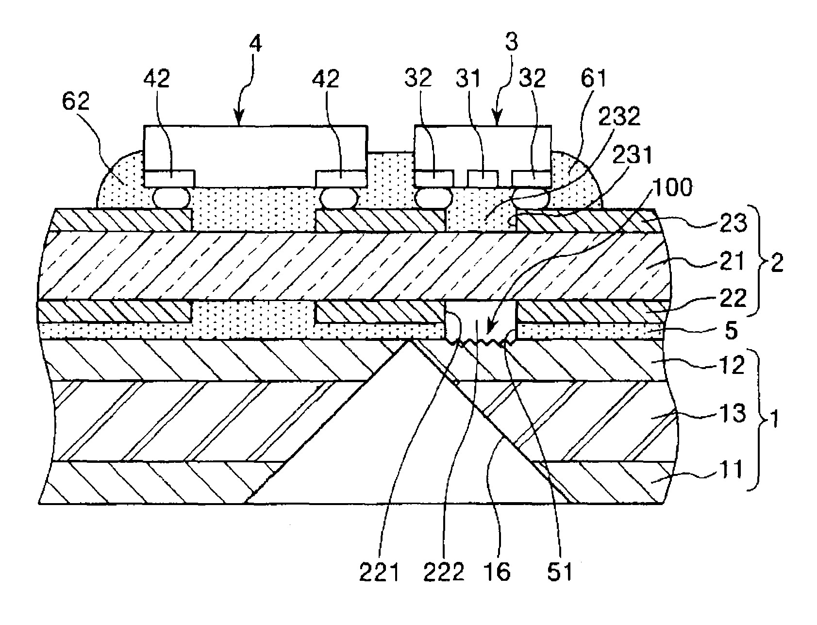
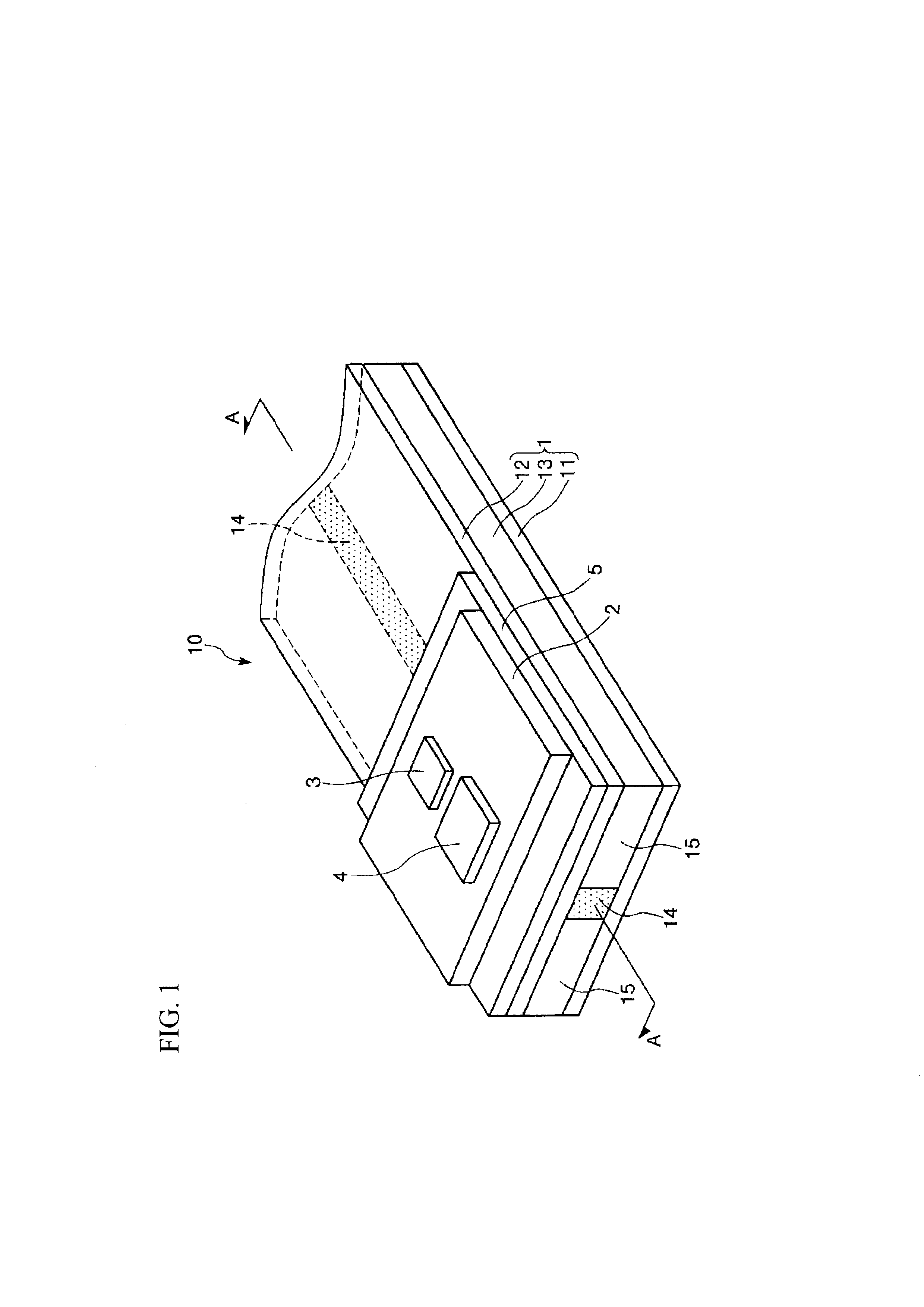
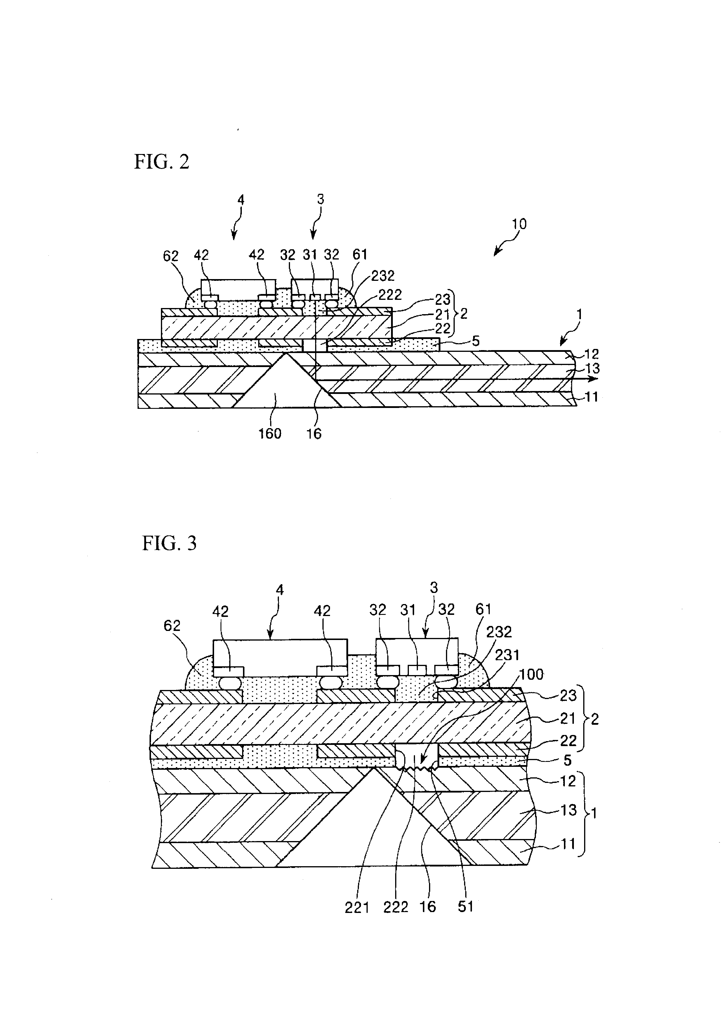
[0104]FIG. 1 shows a perspective diagram illustrating a first embodiment of an optical waveguide module of the invention, FIG. 2 shows a cross-sectional diagram taken along a line A-A of FIG. 1, and FIG. 3 shows a partially enlarged diagram of FIG. 2. In addition, in the following description, an upper side of FIGS. 2 and 3 is referred to as “up” and a lower side is referred to as “down”. In addition, in the respective drawings, a thickness direction is emphatically drawn.

[0105]An optical waveguide module 10 shown in FIG. 1 includes an optical waveguide 1, a circuit board 2 that is provided at an upper side of the optical waveguide 1, and a light-emitting element 3 (optical element) that is mounted on the circuit board 2.

[0106]The optical waveguide 1 has a long...

second embodiment

[0234]Next, a second embodiment of the optical waveguide module of the invention will be described.

[0235]FIG. 10 shows a longitudinal cross-sectional diagram illustrating the second embodiment of the optical waveguide module of the invention.

[0236]Hereinafter, the second embodiment will be described, but the description will be mainly made based on the difference from the first embodiment, and the description of the same matter will be omitted. In addition, in FIG. 10, the above-described reference numerals will be given to the same components as those of the first embodiment, and detailed description thereof will be omitted.

[0237]An optical waveguide module 10 shown in FIG. 10 is the same as the first embodiment except that configurations of the circuit board 2 and the sealing material 61 are different.

[0238]In a circuit board 2 shown in FIG. 10, an opening 211 that penetrates through the insulating substrate 21 is formed in the insulating substrate 21 in correspondence with the op...

third embodiment

[0248]Next, a third embodiment of the optical waveguide module of the invention will be described.

[0249]FIG. 11 shows a longitudinal cross-sectional diagram illustrating the third embodiment of the optical waveguide module of the invention.

[0250]Hereinafter, the third embodiment will be described, but the description will be mainly made based on the difference from the first embodiment, and the description of the same matter will be omitted. In addition, in FIG. 11, the above-described reference numerals will be given to the same components as those of the first embodiment, and detailed description thereof will be omitted.

[0251]An optical waveguide module 10 shown in FIG. 11(a) is the same as the first embodiment except that the optical waveguide module 10 includes a condensing lens 8 that is provided on a lower surface of the insulating substrate 21 so as to protrude into the vacant space 222 and that is different from the lens 100. Due to the condensing lens 8, the signal light th...


PUM


Abstract

An object is to provide an optical waveguide that has low optical coupling loss when optically coupled with an optical element and that is capable of performing high-quality optical communication, a method for efficiently producing the optical waveguide, an optical waveguide module that is provided with the optical waveguide and is capable of performing high-quality optical communication, a method for efficiently producing the optical waveguide module, and an electronic apparatus. Provided is an optical waveguide including: a core portion; a clad portion that is provided to cover a side surface of the core portion; an optical path-converting unit that is provided partway along the core portion or on an extended line of the core portion and that converts an optical path of the core portion to the outside of the clad portion; and a lens that is provided on a surface of the clad portion at least at a portion optically connected to the core portion via the optical path-converting unit, and that is formed by causing the surface to locally protrude or to be locally depressed.

Description

TECHNICAL FIELD [0001]The present invention relates to an optical waveguide, a method for producing the optical waveguide, an optical waveguide module, a method for producing the optical waveguide module, and an electronic apparatus.BACKGROUND ART [0002]In recent years, along with the wave of informatization, the prevalence of broadband lines (broadband), which are capable of communicating large-capacity information at high speed, has increased. In addition, as transmission apparatuses that transmit information to this broadband line, a router apparatus, a WDM (Wavelength Division Multiplexing) apparatus, and the like have been used. A plurality of signal-processing boards, in which a computing device such as an LSI, a storage device such as a memory, and the like are combined, are provided in the transmitting apparatuses and function to mutually connect respective lines.[0003]A circuit, in which the computing device, the storage device, and the like are connected through an electri...

Claims


Application Information

Patent Timeline
IPC IPC(8): G02B6/32G02B6/34
CPCG02B6/4206G02B6/4214G02B6/34G02B6/32G02B6/43
Inventor FUJIWARA, MAKOTOFURUKAWA, TSUYOSHITERADA, SHINSUKEKANETA, MOTOYA
Owner SUMITOMO BAKELITE CO LTD
Learn More