
Method and Apparatus for Use in Improving Linearity of MOSFETs Using an Accumulated Charge Sink

a technology of mosfets and charge sinks, applied in the field of mos field effect transistors, can solve the problems of adversely affecting the linearity adversely affecting the performance of the soi mosfet under certain operating conditions, and adversely affecting the performance of the soi mosfet, so as to improve the nonlinear response and harmonic and intermodulaton distortion effects

Active Publication Date: 2011-07-14
PSEMI CORP
View PDF87 Cites 70 Cited by
  • Summary
  • Abstract
  • Description
  • Claims
  • Application Information

AI Technical Summary

Benefits of technology

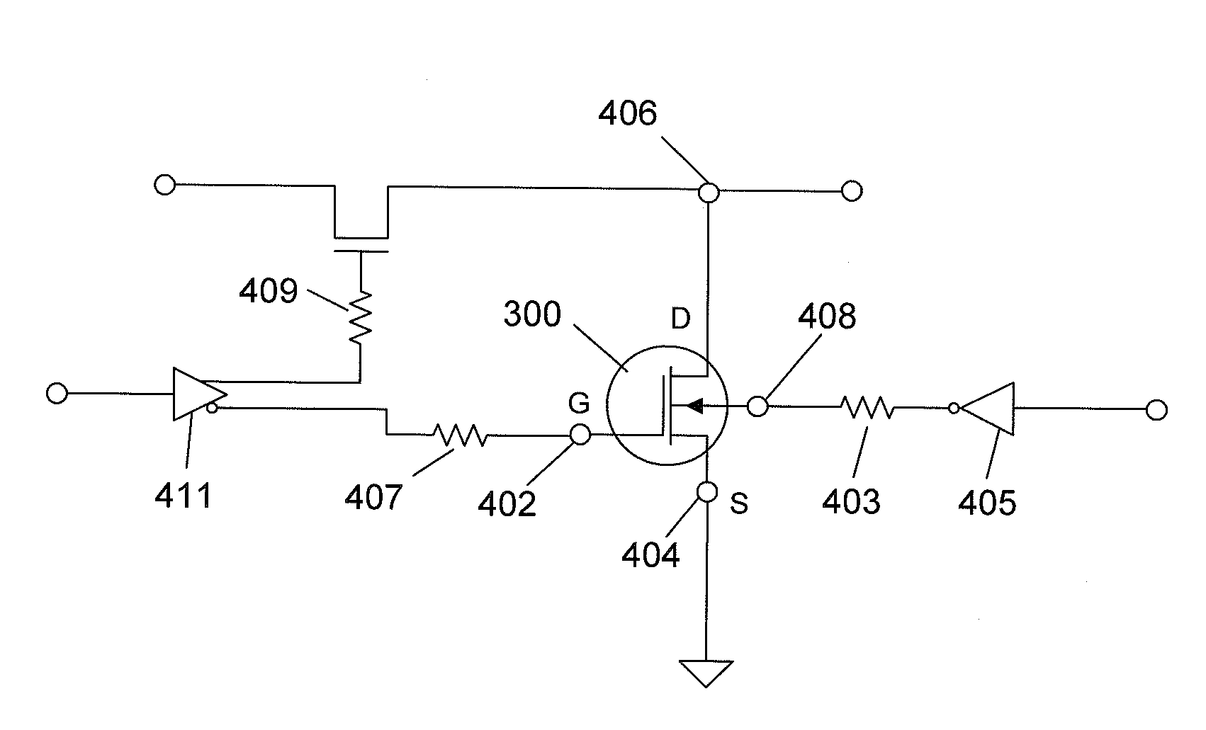
The patent describes a way to control the buildup of charge in MOSFETs to improve their performance. This is done by using a circuit that reduces the nonlinear response and harmonic distortion in the MOSFETs. This circuit includes a device called an accumulated charge sink (ACS) which removes the charge from the MOSFET, reducing its capacitance. The ACS has a high impedance connection to the MOSFET body, which helps to reduce these distortion effects. Overall, this technology improves the accuracy and efficiency of MOSFETs, making them better suited for use in various applications.

Problems solved by technology

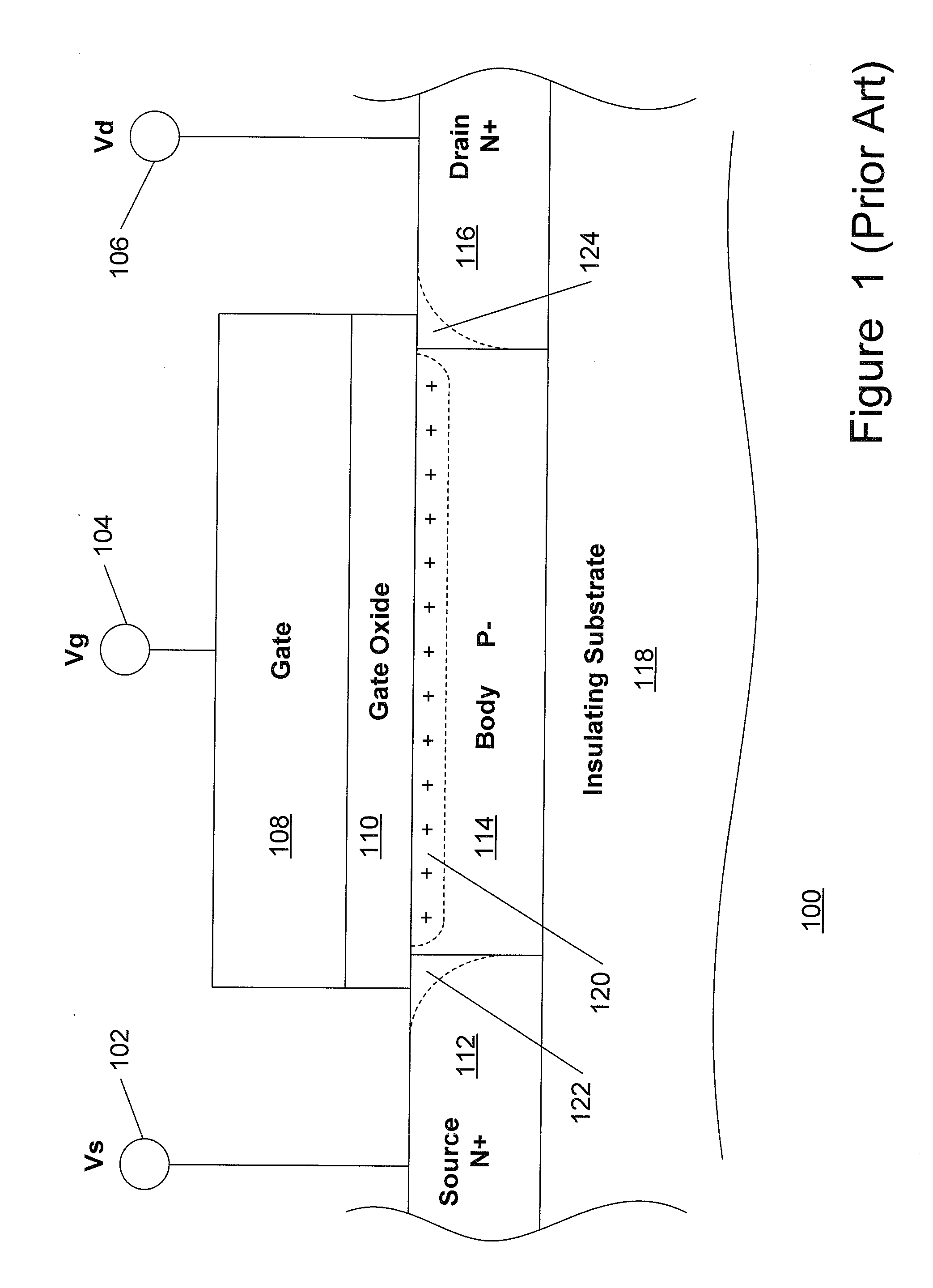
SOI and SOS MOSFETs are often used in applications in which operation within the accumulated charge regime adversely affects MOSFET performance.
As described below in more detail, unless the accumulated charge is removed or otherwise controlled, it detrimentally affects performance of SOI MOSFETs under certain operating conditions.
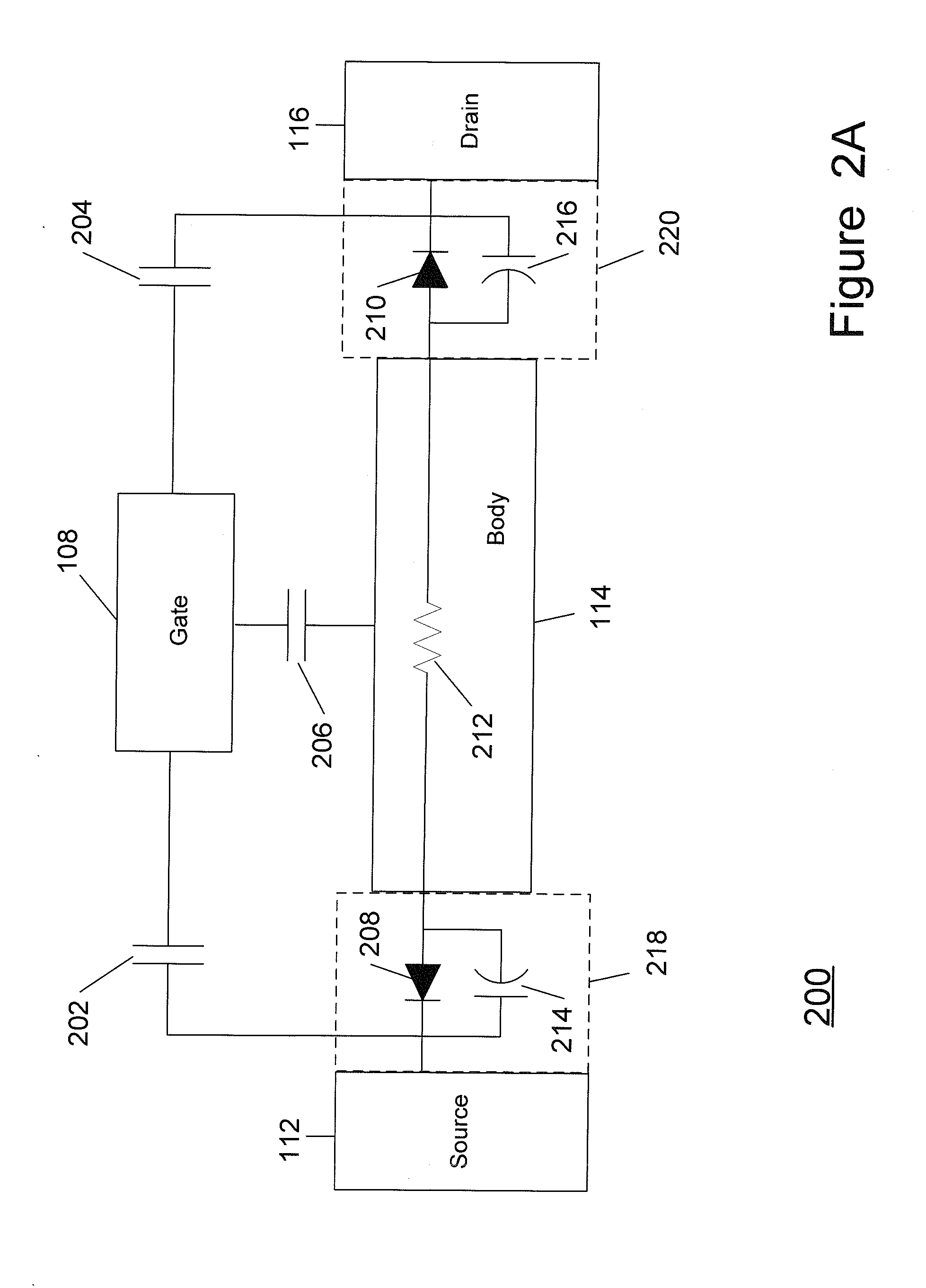
As described below with reference to FIGS. 2B and 5A in more detail, the inventors have discovered that unless the accumulated charge is removed or otherwise controlled, under some operating conditions, the accumulated charge adversely affects the linearity of the SOI MOSFET and thereby increases harmonic distortion and intermodulation distortion (IMD) caused by the MOSFET when used in the implementation of certain circuits.

Method used


Image

  • Method and Apparatus for Use in Improving Linearity of MOSFETs Using an Accumulated Charge Sink
  • Method and Apparatus for Use in Improving Linearity of MOSFETs Using an Accumulated Charge Sink
  • Method and Apparatus for Use in Improving Linearity of MOSFETs Using an Accumulated Charge Sink

Examples


Embodiment Construction

[0055]As noted above, those skilled in the electronic device design arts shall appreciate that the teachings herein apply equally to NMOSFETs and PMOSFETs. For simplicity, the embodiments and examples presented herein for illustrative purposes include only NMOSFETs, unless otherwise noted. By making well known changes to dopants, charge carriers, polarity of bias voltages, etc., persons skilled in the arts of electronic devices will easily understand how these embodiments and examples may be adapted for use with PMOSFETs.

Non-linearity and Harmonic Distortion Effects of Accumulated Charge in an SOI NMOSFET

[0056]As described above in the background, no matter what mode of operation the MOSFET employs (i.e., enhancement mode or depletion mode), under some circumstances, when a MOSFET is operated in an off-state with a nonzero gate bias voltage applied with respect to the source and drain, an accumulated charge may occur under the gate. According to the present teachings, as described a...


PUM


Abstract

A method and apparatus for use in improving the linearity characteristics of MOSFET devices using an accumulated charge sink (ACS) are disclosed. The method and apparatus are adapted to remove, reduce, or otherwise control accumulated charge in SOI MOSFETs, thereby yielding improvements in FET performance characteristics. In one exemplary embodiment, a circuit having at least one SOI MOSFET is configured to operate in an accumulated charge regime. An accumulated charge sink, operatively coupled to the body of the SOI MOSFET, eliminates, removes or otherwise controls accumulated charge when the FET is operated in the accumulated charge regime, thereby reducing the nonlinearity of the parasitic off-state source-to-drain capacitance of the SOI MOSFET. In RF switch circuits implemented with the improved SOI MOSFET devices, harmonic and intermodulation distortion is reduced by removing or otherwise controlling the accumulated charge when the SOI MOSFET operates in an accumulated charge regime.

Description

CROSS-REFERENCE TO RELATED APPLICATIONSClaim of Priority[0001]This application is a divisional application of commonly assigned U.S. application Ser. No. 11 / 484,370, “Method and Apparatus for use in Improving Linearity of MOSFETs Using an Accumulated Charge Sink”, filed Jul. 10, 2006, issuing Mar. 22, 2011 as U.S. Pat. No. 7,910,993; and co-pending application Ser. No. 11 / 484,370 claims the benefit of priority under 35 U.S.C. §119 (e) to commonly-assigned U.S. Provisional Application No. 60 / 698,523, filed Jul. 11, 2005, entitled “Method and Apparatus for use in Improving Linearity of MOSFETs using an Accumulated Charge Sink” (ATTY. DOCKET NO. PER-016-PROV); this divisional application is also related to commonly assigned U.S. application Ser. No. 11 / 520,912 filed Sep. 14th, 2006 which issued Feb. 15th, 2011 as U.S. Pat. No. 7,890,891, and which 11 / 520,912 application (and now issued patent) is a continuation-in-part of U.S. application Ser. No. 11 / 484,370, filed Jul. 10, 2006 (issui...

Claims


Application Information

Patent Timeline
Patent Type & Authority Applications(United States)
IPC IPC(8): H03K17/687H01L29/78H03K3/01
CPCH01L29/78609H01L29/78615H03K17/162H01L29/78684H03K2217/0018H01L29/78681H01L29/0649H01L29/1095H03K17/687
Inventor BRINDLE, CHRISTOPHER N.STUBER, MICHAEL A.KELLY, DYLAN J.KEMERLING, CLINT L.IMTHURN, GEORGE P.WELSTAND, ROBERT B.BURGENER, MARK L.
Owner PSEMI CORP
Learn More