Pixel structure of electroluminescent display panel
a technology pixel structure, which is applied in the field of pixel structure can solve the problems of voltage drop, uneven image, voltage drop, etc., and achieve the effect of avoiding voltage signal drop and avoiding uneven display image of electroluminescent display panel
- Summary
- Abstract
- Description
- Claims
- Application Information
AI Technical Summary
Benefits of technology
Problems solved by technology
Method used
Image

Examples
first embodiment
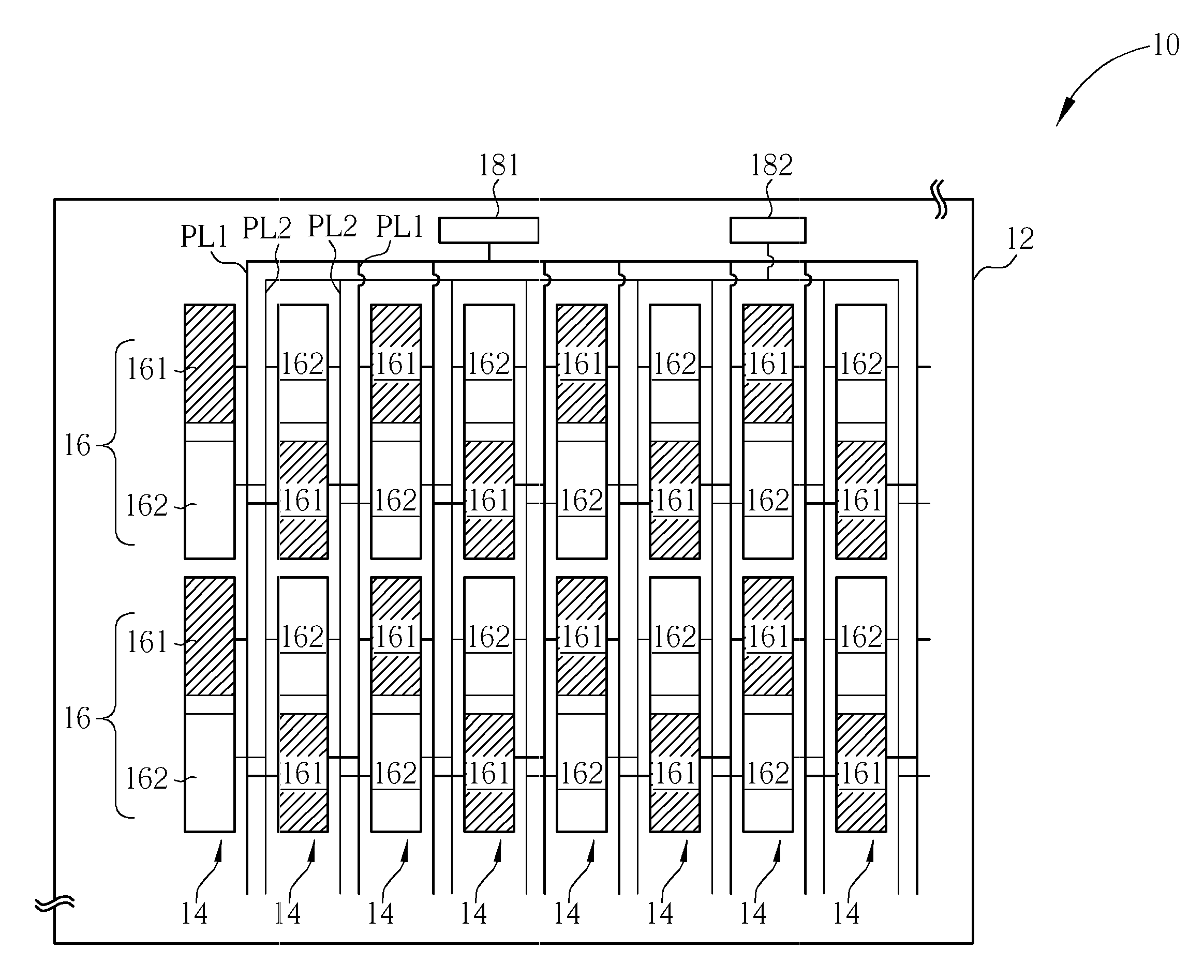
[0017]Referring to FIG. 1, FIG. 1 is a schematic diagram illustrating a pixel structure of an electroluminescent display panel in accordance to the present invention. As illustrated in FIG. 1, the pixel structure 10 of the electroluminescent display panel in accordance to the present embodiment is disposed on a substrate 12, and the pixel structure 10 includes a plurality of sub-pixel columns 14, a plurality of first power lines PL1 and a plurality of second power lines PL2. The sub-pixel columns 14 in accordance to the present embodiment is a collection of sub-pixels aligned along a column direction (a perpendicular direction) of FIG. 1. Each of the sub-pixel columns 14 includes a plurality of sub-pixels 16, and each of the sub-pixels 16 at least includes a first sub-pixel 161 and a second sub-pixel 162. The first sub-pixel 161 and the second sub-pixel 162 are used to display the same sub-pixel frame, but the first sub-pixel 161 and the second sub-pixel 162 are electrically insulat...
third embodiment
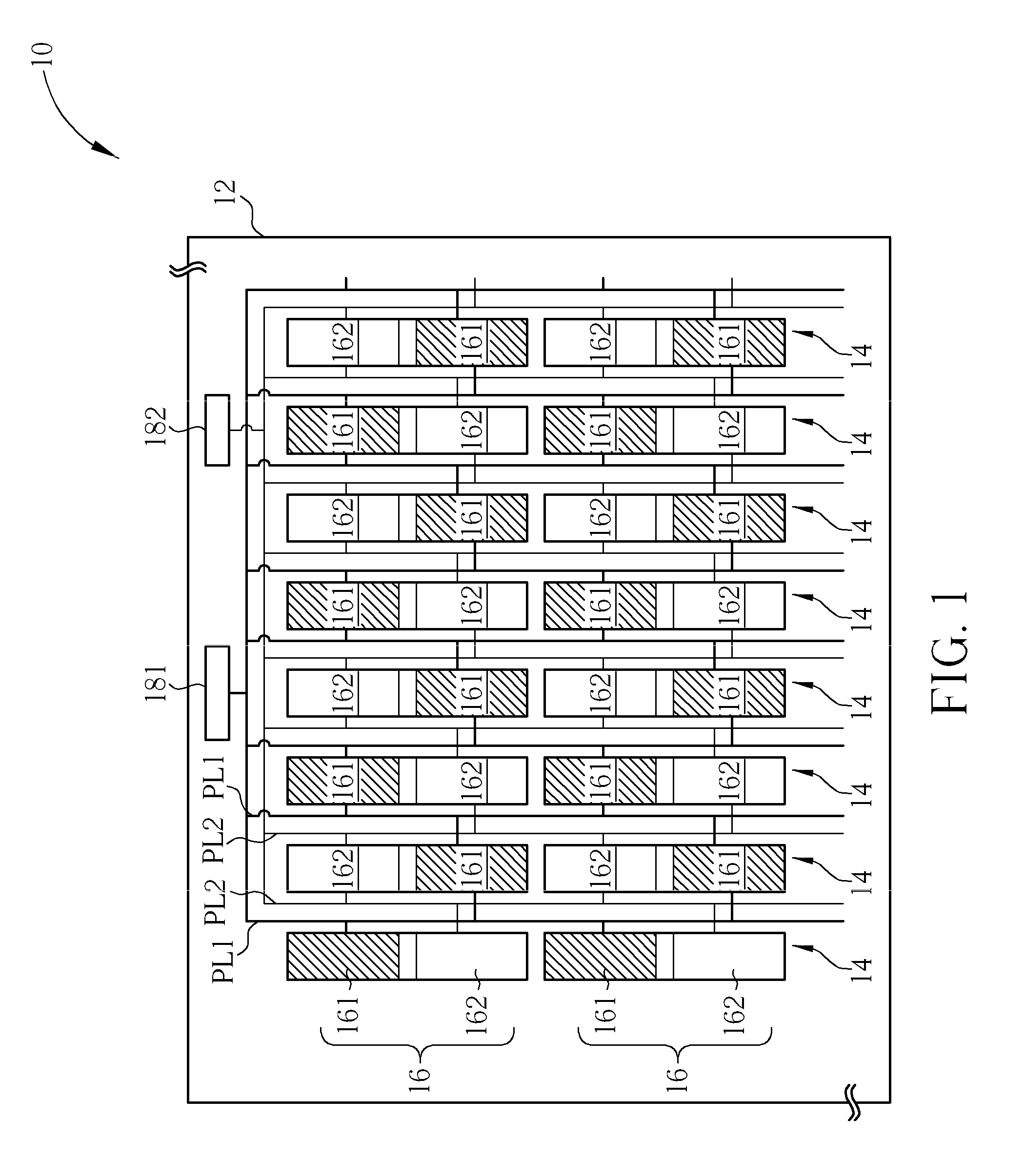
[0023]Referring to FIG. 4, FIG. 4 is a schematic diagram illustrating a pixel structure of an electroluminescent display panel in accordance to the present invention. As illustrated in FIG. 4, in a pixel structure 40 of an electroluminescent display panel in accordance to the present embodiment, the sub-pixels 16 of a same sub-pixel column 14 have a same display color, but the sub-pixels 16 of two adjacent sub-pixel columns 14 have different display colors. Different from the first preferred embodiment, each of the sub-pixels 16 in accordance to the present embodiment does not further include a first sub-pixel and a second sub-pixel. Furthermore, the nth first power line PL1 is disposed between the sub-pixel column 14 of the 2nth column and the sub-pixel column 14 of the (2n+1)th column, and the nth second power line PL2 is disposed between the sub-pixel column 14 of the 2nth column and the sub-pixel column 14 of the (2n+1)th column, where n is an integer grater than or equal to 1. ...
PUM
 Abstract
Description
Claims
Application Information
 - R&D
- Intellectual Property
- Life Sciences
- Materials
- Tech Scout
- Unparalleled Data Quality
- Higher Quality Content
- 60% Fewer Hallucinations
Browse by: Latest US Patents, China's latest patents, Technical Efficacy Thesaurus, Application Domain, Technology Topic, Popular Technical Reports.
© 2025 PatSnap. All rights reserved.Legal|Privacy policy|Modern Slavery Act Transparency Statement|Sitemap|About US| Contact US: help@patsnap.com