Method for integrated circuit design verification in a verification environment

a verification environment and integrated circuit technology, applied in the direction of instruments, specific program execution arrangements, program control, etc., can solve the problems of difficult to observe sections in hardware description language, thorough testing, and take a lot of time, so as to improve the quality of ics or fpga, improve the quality of design testing, and reduce the time required for generating test cases.

Inactive Publication Date: 2011-03-03
VENELL MARTTI
View PDF13 Cites 34 Cited by
  • Summary
  • Abstract
  • Description
  • Claims
  • Application Information

AI Technical Summary

Benefits of technology

[0030]The benefits of the invention is related to improved testing of designs, which further provides improved quality of ICs or FPGA. With the invention there may be fewer bugs ...

Problems solved by technology

The problem in existing testing systems is that a user must manually define test case data, which takes a lot of time.
In manual table testing it may be difficult to observe sections in hardware description language that are possible sou...

Method used


Image

  • Method for integrated circuit design verification in a verification environment
  • Method for integrated circuit design verification in a verification environment
  • Method for integrated circuit design verification in a verification environment

Examples


Embodiment Construction

[0036]Reference will now be made in detail to the embodiments of the present invention, examples of which are illustrated in the accompanying drawings.

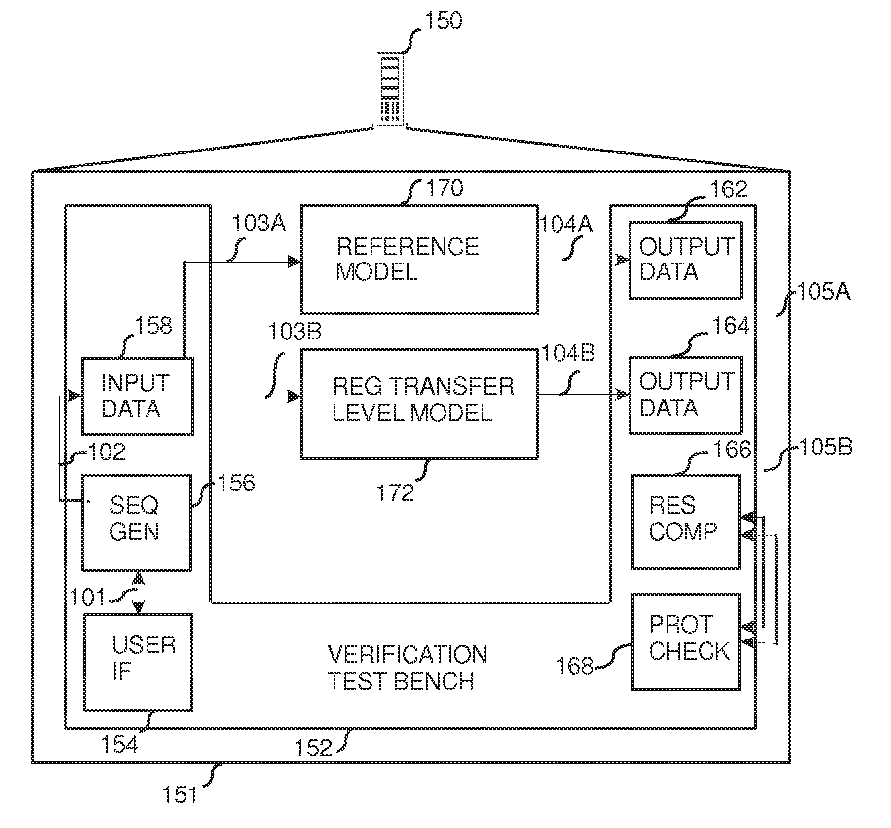
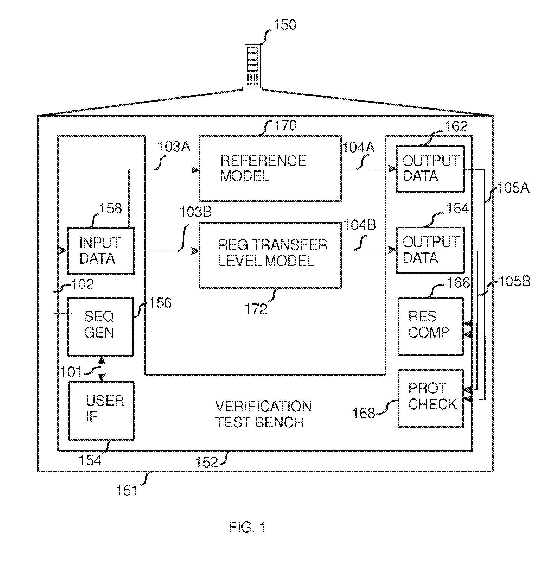
[0037]FIG. 1 is a block diagram illustrating design verification environment in one embodiment of the invention. In FIG. 1 there is illustrated an apparatus 150, which comprises at least one processor and at least one memory. The at least one memory comprises a primary memory and a secondary memory. The primary memory is, for example, a Random Access Memory (RAM). The secondary memory may be, for example, a magnetic disk, an optic disk, a magneto-optic disk or a flash-memory. The internal functions of apparatus 150 are illustrated with a box 151. The at least one memory in apparatus 150 is configured to store a verification test bench 152. Verification test bench 152 comprises a user interface entity 154, a sequence generation entity 156, a result comparison entity 166 and a protocol checking entity 168. Verification test bench 152 pr...


PUM


Abstract

The invention relates to a method. In the method a reference model and a register transfer level model are obtained to a test bench. To a user is presented at least one wave diagram in a user interface on a display of an apparatus. A time interval associated with an input vector is determined based on a first type of user input. A random number range is associated with the time interval based on a second type of user input. The generation of an input data file is started for at least one test case for the reference model and the register transfer level model. Random numbers within the random number range are generated, the random numbers being stored within the input data file. The test cases are executed using either of the models.

Description

BACKGROUND OF THE INVENTION[0001]1. Field of the Invention[0002]The invention relates to Integrated Circuits (IC) design and development. Particularly, the invention relates to a method for integrated circuit design verification in a verification environment.[0003]2. Description of the Related Art[0004]Integrated Circuits (IC) are manufactured on the surface of a semiconductor substrate material. The manufacturing is based on imaging, deposition and etching steps where patterns from predesigned photo masks are projected on a light-sensitive chemical resist on the surface to produce an exposure pattern. Thereupon, chemical processes are applied to engrave the exposure pattern into the substrate underneath the photo resist. A semiconductor wafer may undergo dozens of photolithographic cycles. The photo masks are produced by printing graphical models of different layers of the circuit. The graphical models in turn may be produced from a logical model of the circuit. In order to avoid p...

Claims


Application Information

Patent Timeline
IPC IPC(8): G06F9/455
CPCG01R31/318364
Inventor VENELL, MARTTI
Owner VENELL MARTTI
Why Eureka
Try Eureka