Method and system of finding a read voltage for a flash memory
a flash memory and optimal reading technology, applied in the field of flash memory, can solve problems such as the possibility of changing the threshold voltage distribution, and achieve the effect of reducing the error bit number
- Summary
- Abstract
- Description
- Claims
- Application Information
AI Technical Summary
Benefits of technology
Problems solved by technology
Method used
Image
Examples
first embodiment
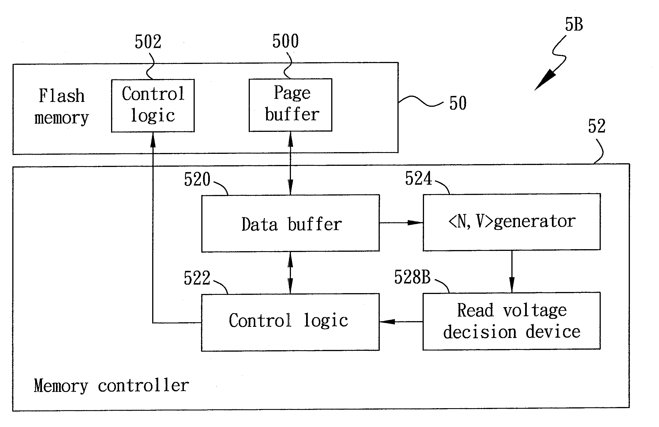
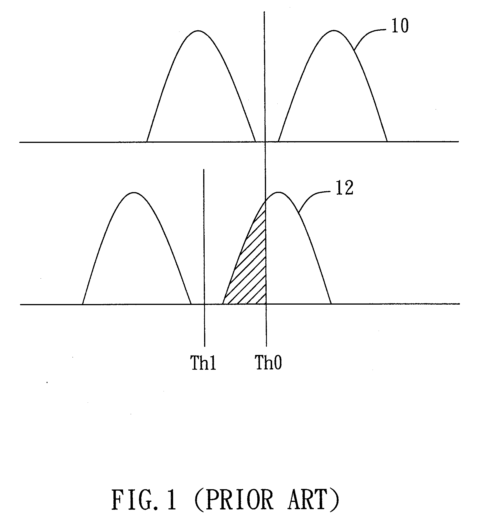
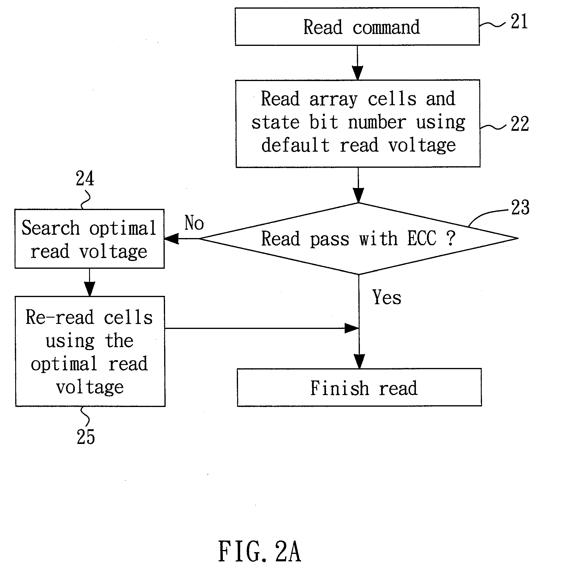
[0026]FIG. 3A shows a detailed flow diagram of the step 24 (of FIG. 2A or FIG. 2B) for determining the optimal read voltage according to the present invention. In the embodiment, a page (or any specific amount) is read from the flash memory many times using multiple read voltages respectively (the step 241). Next, in the step 242, the (cumulative) bit numbers (e.g., N1, N2, etc.) respectively corresponding to the read voltages (e.g., V1, V2, etc.) are counted, for example, as 1,V1>, 2,V2>, etc. Subsequently, in the step 243, an optimal read voltage or offset voltage is determined according to a predetermined lookup table (LUT) that maps a failure ratio (or a failure bit number) to a read voltage (or offset voltage). FIG. 3B illustrates the concept of the failure bit number. As shown in the figure, the recorded (cumulative) bit number of state “1” using a default read voltage V0 is n, and the counted (cumulative) bit number of the state “1” using the read voltage V1 is N1. Therefore,...
second embodiment
[0029]FIG. 4A shows a detailed flow diagram of the step 24 (of FIG. 2A or FIG. 2B) for determining the optimal read voltage according to the present invention. The flow diagram in FIG. 4A is similar to that in FIG. 3A except that the step 243 is now replaced with the step 244, in which the optimal read voltage is determined according to at least two sets of the recorded state bit number (during the programming) and the counted bit number (during the reading). For example, n1 is the recorded bit number for the state “1,” N1 is the first counted bit number for the state “1” using a first read voltage V1, and N2 is the second counted bit number for the state “1” using a second read voltage V2. FIG. 4B shows an example in which the Y axis represents the counted state bit number minus the recorded state bit number, and the X axis represents the associated read voltage. The optimal interpolated read voltage Vtarget between V1 and V2 has a state bit number equal to the counted state bit nu...
PUM
 Abstract
Description
Claims
Application Information
 - R&D
- Intellectual Property
- Life Sciences
- Materials
- Tech Scout
- Unparalleled Data Quality
- Higher Quality Content
- 60% Fewer Hallucinations
Browse by: Latest US Patents, China's latest patents, Technical Efficacy Thesaurus, Application Domain, Technology Topic, Popular Technical Reports.
© 2025 PatSnap. All rights reserved.Legal|Privacy policy|Modern Slavery Act Transparency Statement|Sitemap|About US| Contact US: help@patsnap.com


