Method and device for hitless tunable optical filtering

Active Publication Date: 2010-08-05
GOOGLE LLC
View PDF29 Cites 11 Cited by
  • Summary
  • Abstract
  • Description
  • Claims
  • Application Information

AI Technical Summary

Benefits of technology

[0011]The Applicant has found that there is a need for an optical communication system having tunable optical processing functionality which leaves unaltered, or at least reduces the alteration of, the thru channels during tuning, i.e. it should be ideally hitless. In addition, the optical processing node should preferably be low-loss, low-cost, fast tunable and / or broadband.
[0013]The Applicant has found a method and a system for optical transmission provided with tunable optical processing functionality which can solve one or more of the problems stated above. The solution of the present invention is simple, feasible and low cost.

Problems solved by technology

The Applicant has noted that the filter devices described in the above cited articles are not optimally designed and / or operated for changing (tuning) the filtered optical channel from an initial channel to a final one while keeping at zero or low level the power and / or dispersion hit on the thru channels (placed in between the initial and final channel and / or outside the spectral region spanning from the initial to the final channel) during the entire tuning procedure.

Method used


Image

  • Method and device for hitless tunable optical filtering
  • Method and device for hitless tunable optical filtering
  • Method and device for hitless tunable optical filtering

Examples


Embodiment Construction

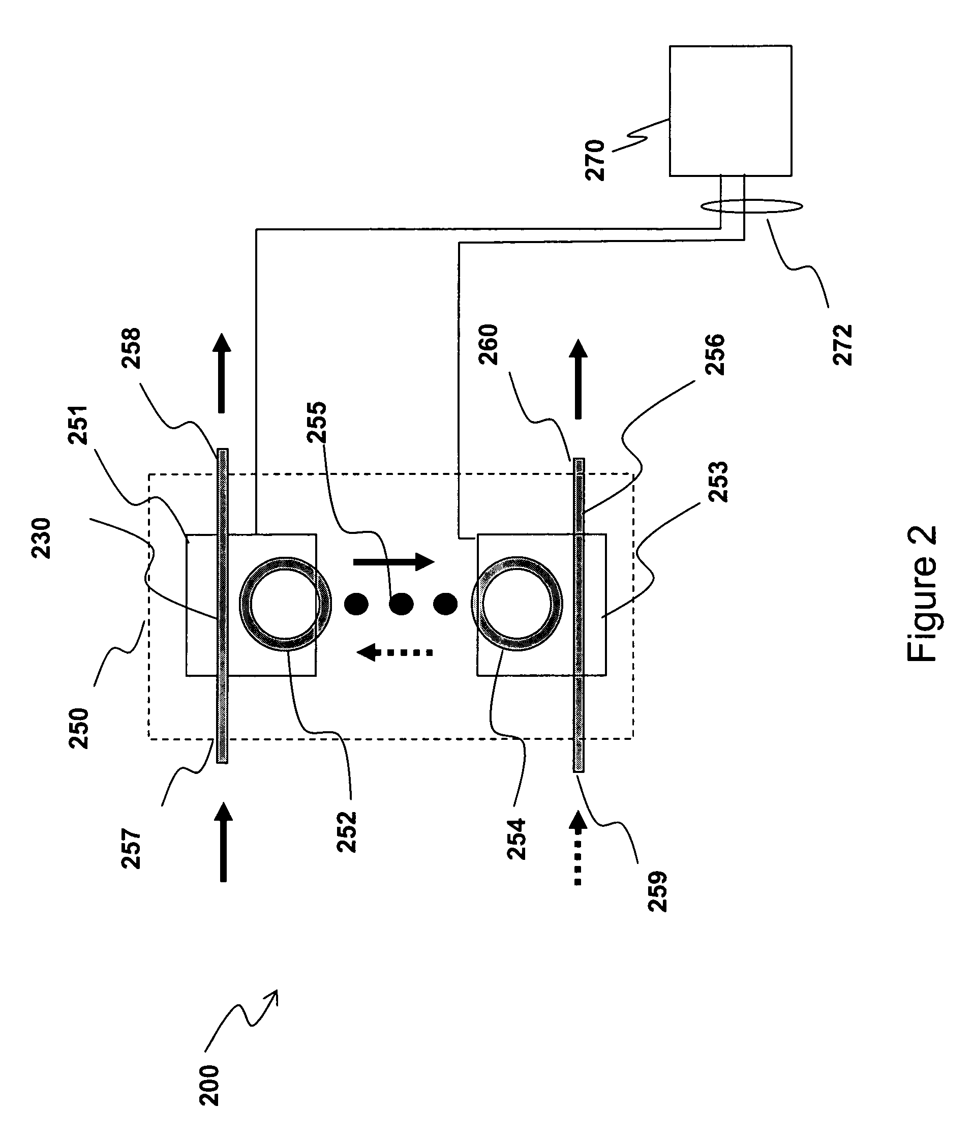
[0038]FIG. 1 shows an optical communication system architecture according to a possible embodiment of the present invention.

[0039]The optical communication system 100 comprises at least a transmitter 110, a receiver 120 and an optical line 130 which optically connects the transmitter and the receiver. The transmitter 110 is an opto-electronic device apt to emit an optical signal carrying information. It typically comprises at least an optical source (e.g., a laser) apt to emit an optical radiation and at least a modulator apt to encode information onto the optical radiation. Preferably, the transmitter 110 is a WDM transmitter (e.g., a DWDM transmitter) and the optical signal may comprise a plurality of optical channels (each carrying modulation-encoded information) having respective optical frequencies equally spaced by a given frequency spacing and occupying an optical bandwidth. Preferably, said optical signal lies in the near-infrared wavelength range, e.g. from 900 nm to 1700 n...


PUM


Abstract

The method for filtering an optical signal comprising a plurality of channels lying on a grid of optical frequencies equally spaced by a frequency spacing and occupying an optical bandwidth, comprises: a) operating an optical filter comprising a plurality of resonators, wherein a first resonator of the plurality is optically coupled to the optical signal and the remaining resonators are optically coupled in series to the first resonator, so that a respective resonance of each one of the plurality of resonators falls within a first frequency band having bandwidth less than or equal to 15 GHz; b) operating the optical filter so as to obtain a separation between said respective resonance of at least one resonator with respect to said respective resonance of at least another different resonator, the separation being greater than or equal to 25 GHz; c) operating the optical filter so that said respective resonance of each one of the plurality of resonators falls within a second frequency band, different from the first frequency band, having bandwidth less than or equal to 15 GHz, wherein during the procedure from step a) to step c), at least one among said respective resonance of the at least one resonator and said respective resonance of the at least another different resonator is moved also outside a frequency region spanning between, and including, the first and the second frequency band. A corresponding device for filtering an optical signal is disclosed.

Description

FIELD OF THE INVENTION[0001]The present invention relates to the field of optical communication systems including hitless tunable optical filtering functionality, such as hitless tunable optical add and / or drop functionality.BACKGROUND OF THE INVENTION[0002]A common technique to increase the transmission capacity of today optical communication systems is wavelength division multiplexing (WDM), wherein a plurality of optical channels, each having a respective optical frequency (and correspondingly respective optical wavelength), are multiplexed together in a single optical medium, such as for example an optical fiber. The optical frequencies allocated for the WDM channels are typically arranged in a grid having an equal spacing between two adjacent frequencies. In dense WDM (DWDM), wherein the WDM channels may be closely spaced, the frequency spacing is typically equal to about 100 GHz (corresponding to a wavelength spacing of about 0.8 nm in the near infrared band—roughly between 1 ...

Claims


Application Information

Patent Timeline
IPC IPC(8): H04B10/12G02B6/26
CPCG02B6/12007G02B6/29343G02B6/29383H04J14/0212H04J14/0206H04J14/021G02B6/29395
Inventor BOLLA, LORENZOGALLI, PAOLAGHIDINI, SILVIAROMAGNOLI, MARCOSOCCI, LUCIANO
Owner GOOGLE LLC
Why Eureka
Try Eureka