Metal substrate having electronic devices formed thereon

a metal substrate and electronic device technology, applied in the field of electronic devices fabricated on metal substrates, can solve the problems of limited substrate material range that has been used successfully, form and manage limitations, and frustrate efforts to fabricate larger displays and devices, and achieve the effect of high degree of smoothness

Inactive Publication Date: 2010-05-27
CARESTREAM HEALTH INC
View PDF15 Cites 0 Cited by
  • Summary
  • Abstract
  • Description
  • Claims
  • Application Information

AI Technical Summary

Benefits of technology

[0012]It is an advantage of the present invention that it provides a thin metal substrate having a high degree of smoothness without the need for extensive surface treatment.

Problems solved by technology

Thus, the range of substrate materials that have been used successfully is somewhat limited, generally to glass, quartz, or other rigid, silicon-based materials.
Among other problems, the limitations inherent to these substrates frustrate efforts to fabricate larger displays and devices, since crystalline silicon and many types of glass that are conventionally employed as substrates become increasingly difficult to form and manage in large, thin, lightweight sheets.
However, problems with surface morphology, resulting in increased capacitive coupling, edge effects, and possible shorting between layered components formed thereon, make metal foil substrates difficult to fabricate for use with AMOLED or other thin-film devices.
Thus, while they exhibit many desirable properties and offer significant potential for lightweight component designs, metal substrates have yet to be shown as practical replacements for glass or silicon wafer materials.
One major hurdle with conventional approaches to providing and preparing a metal substrate suitable for thin-film device fabrication thereon relates to surface characteristics using existing surface treatment techniques.
Any rougher surface would require an excessively thick planarization layer, more likely subject to cracking and other defects.
While there are adaptable wafer-surface treatment techniques for smoothing the surface, such as chemical-mechanical polishing (CMP), such techniques are very costly and are limited in treatment surface area.
Another difficulty with conventional techniques are relatively high defect rates.

Method used


Image

  • Metal substrate having electronic devices formed thereon
  • Metal substrate having electronic devices formed thereon
  • Metal substrate having electronic devices formed thereon

Examples


Embodiment Construction

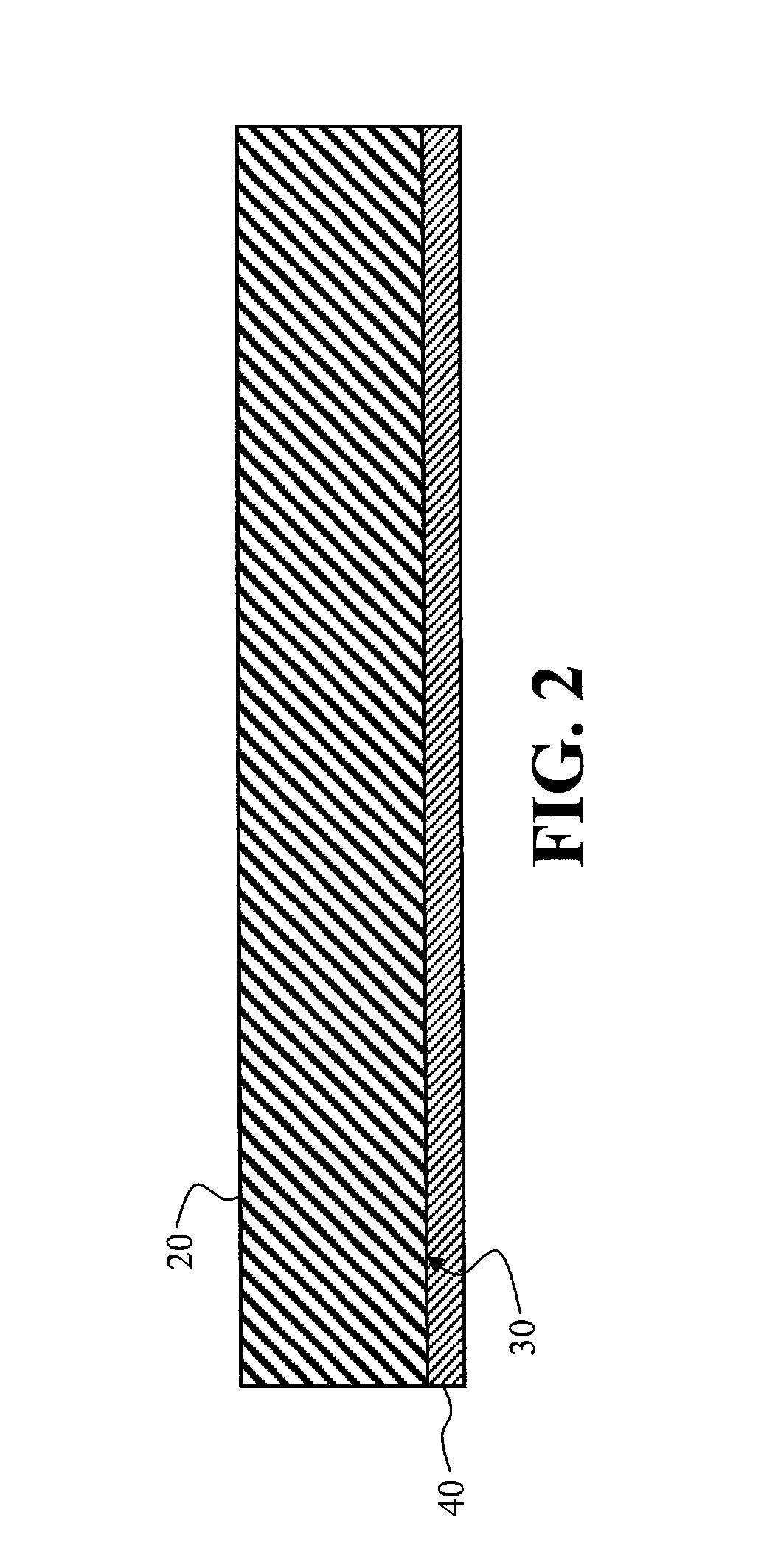
[0030]The method of the present invention allows the formation of thin-film electronic devices on a metal substrate by first forming a seed layer by depositing metal onto a very smooth master surface. One or more successive metals layers are then bonded to this seed layer as support structure. The multi-layered metal substrate that is thus formed can then be detached from the master to provide the smooth surface necessary for TFT fabrication.

[0031]Figures showing the various layers and structures used for the present invention are not to scale, but exaggerate relative thicknesses of various components for clarity of description.

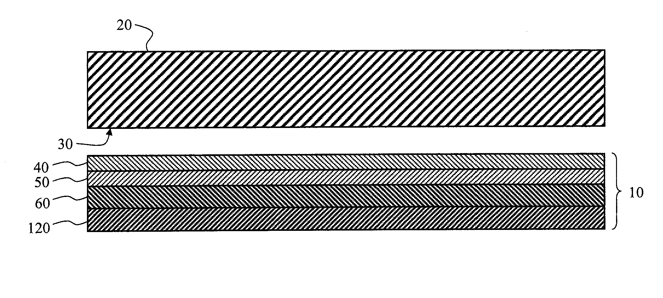
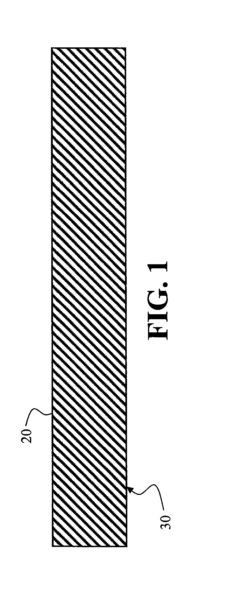
[0032]The cross-sectional views of FIGS. 1 through 5 show, in sequence, a series of processes used to form a substrate having an electronic device 100. FIG. 1 is a cross section view showing a master 20 with a master surface 30. Master 20 is a material such as glass, quartz, or a metal having a highly polished surface 30 with a surface roughness of less than ...


PUM

PropertyMeasurementUnit
roughnessaaaaaaaaaa
thicknessesaaaaaaaaaa
smoothnessaaaaaaaaaa

Abstract

A method of forming an electronic device on a metal substrate deposits a first seed layer of a first metal on at least one master surface with a roughness less than 400 nm. A supporting metal layer is bonded to the first seed layer to form the metal substrate 10. The metal substrate is removed from the master surface, and at least one electronic device is formed on the seed layer of the metal substrate.

Description

CROSS REFERENCE TO RELATED APPLICATIONS[0001]This is a Continuation of U.S. Ser. No. 11 / 553,018 filed on Oct. 26, 2006, entitled METAL SUBSTRATE HAVING ELECTRONIC DEVICES FORMED THEREON, by Kerr et al.[0002]Reference is made to U.S. Ser. No. ______ filed on even date, entitled METAL SUBSTRATE HAVING ELECTRONIC DEVICES FORMED THEREON, by Kerr et al. which is also a Continuation of U.S. Ser. No. 11 / 553,018 filed on Oct. 26, 2006, entitled METAL SUBSTRATE HAVING ELECTRONIC DEVICES FORMED THEREON, by Kerr et al., published as US 2008 / 0115350, incorporated herein by reference.[0003]Reference is made to U.S. patent application Ser. No. 11 / 461,080, filed Jul. 31, 2006, entitled FLEXIBLE SUBSTRATE WITH ELECTRONIC DEVICES FORMED THEREON, by Tredwell at al., published as US 2008 / 0026581, the disclosure of which is incorporated herein.FIELD OF THE INVENTION[0004]This invention generally relates to electronic devices and more particularly relates to electronic device fabricated on a metal subst...

Claims


Application Information

Patent Timeline
Patent Type & Authority Applications(United States)
IPC IPC(8): H01L21/334
CPCH01L27/1214H01L27/1266H01L29/78603Y10T29/4913Y10T29/49155Y10T29/49128Y10T29/49126H01L21/84
Inventor KERR, ROGER S.TREDWELL, TIMOTHY J.HARLAND, MARK A.
Owner CARESTREAM HEALTH INC
Why Eureka
Try Eureka