
Reaction chamber

a technology of reaction chamber and substrate, which is applied in the direction of coating, chemical vapor deposition coating, metallic material coating process, etc., can solve the problems of reducing and affecting the uniformity of deposition across the surface of the substra

Inactive Publication Date: 2010-05-13
ASM AMERICA INC
View PDF31 Cites 318 Cited by
  • Summary
  • Abstract
  • Description
  • Claims
  • Application Information

AI Technical Summary

Benefits of technology

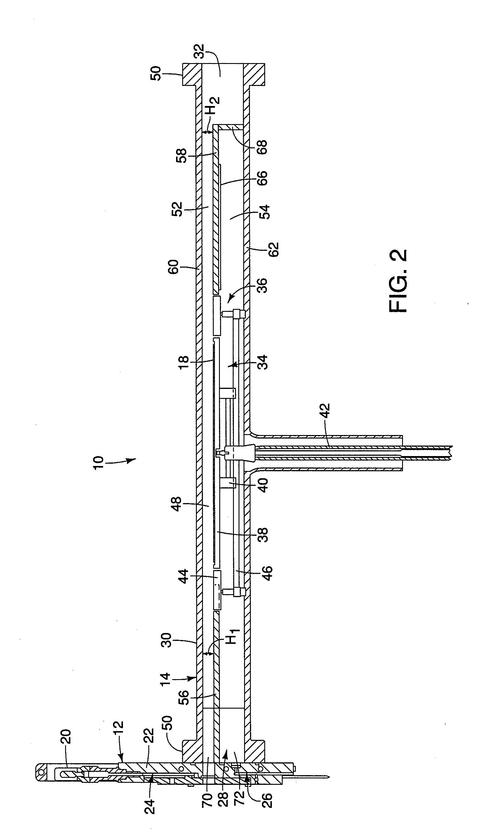
[0010] In one aspect of the present invention, a reaction chamber is provided. The reaction includes an upper chamber having a stationary upper wall and a first inlet in fluid communication with the upper chamber. The first inlet is configured to allow at least one gas to be introducible into the upper chamber. The reaction chamber also includes a lower chamber having a lower wall. The lower chamber is in fluid communication with the upper chamber. The reaction chamber further includes a plate separating at least a portion of the upper chamber and at least a portion of the lower chamber. The plate is spaced apart from the upper wall by a first distance, and the plate is spaced apart from the lower wall by a second distance. An outlet is disposed opposite the first inlet. The upper chamber is tunable for producing a substantially stable and laminar flow of gases between the first inlet and the outlet by adjusting the first distance.
[0012] In still another aspect of the present invention, a reaction chamber is provided. The reaction chamber includes an upper wall, a lower wall, and a pair of opposing side walls connecting the upper and lower walls to define a reaction space therewithin. An inlet is located at one end of the reaction space, and an outlet is located at an opposing end of the reaction space. A velocity of at least one gas flowing through the reaction space is tunable by adjusting the upper wall relative to the lower wall to produce substantially stable and laminar flow of the at least one gas through the reaction space.
[0013] In yet another aspect of the present invention, a reaction chamber is provided. The reaction chamber includes a reaction space in which a substrate is supportable, and the reaction space has a volume. The reaction chamber also includes an inlet through which at least one gas is introducible into the reaction space, and an outlet through which gases within the reaction space exit the reaction space. The volume is tunable to provide substantially stable and laminar flow of gases through the reaction space.

Problems solved by technology

When these localized areas of turbulence overlap with the surface of the substrate being processed, the uniformity of deposition across the surface of the substrate worsens.
The localized areas of turbulence of the process gases that react with the substrate may cause bumps, ridges, or other localized deposition formations that reduce the uniformity of deposition.
The profile of the surface of the substrate after deposition can be unpredictable due in part to the non-laminar and unstable flow of gases through the reaction chamber.

Method used


Image

  • Reaction chamber
  • Reaction chamber
  • Reaction chamber

Examples


Embodiment Construction

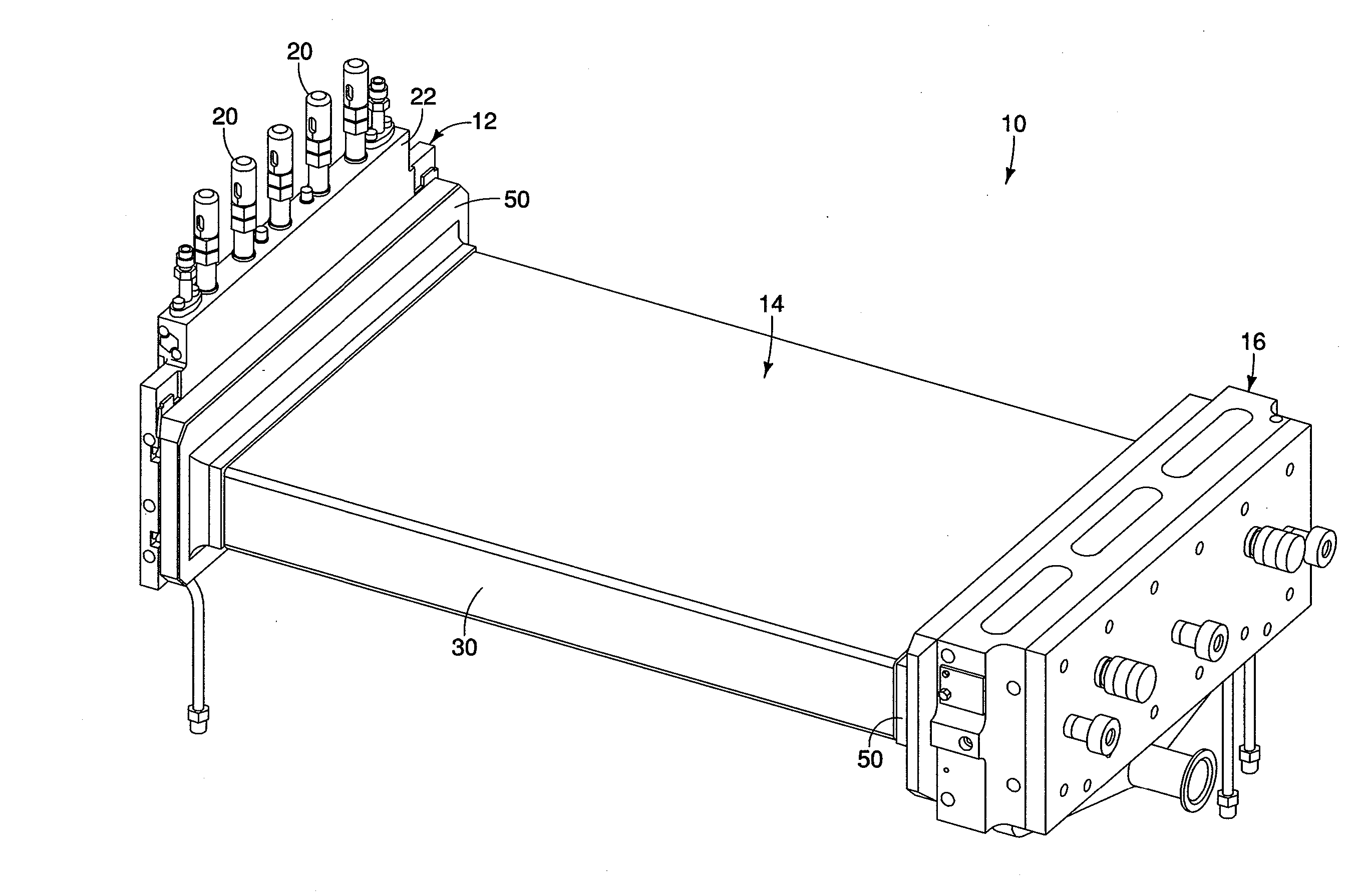
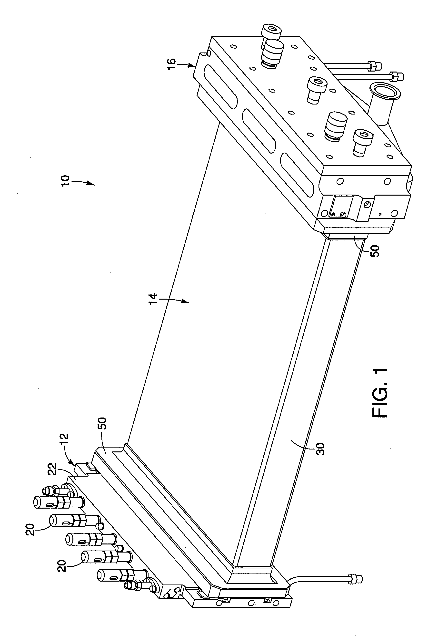
[0025] Referring to FIG. 1, an exemplary embodiment of a semiconductor processing system 10 is shown. The semiconductor processing system 10 includes an injector assembly 12, a reaction chamber assembly 14, and an exhaust assembly 16. The semiconductor processing system 10 is configured to receive a substrate 18 (FIG. 2) to be processed within the reaction chamber assembly 14. The injector assembly 12 is configured to introduce various gases into the reaction chamber assembly 14, wherein at least one chemical reaction takes place within the reaction chamber assembly 14 between the gases introduced therein and the substrate 18 being supported therein. The unreacted process gases as well as the exhaust gases are then removed from the reaction chamber assembly 14 through the exhaust assembly 16.

[0026] As shown in FIGS. 1-2, an embodiment of the injector assembly 12 includes a plurality of injectors 20 operatively connected to an inlet manifold 22. In an embodiment, the inlet manifold ...


PUM

PropertyMeasurementUnit
velocityaaaaaaaaaa
velocityaaaaaaaaaa
widthaaaaaaaaaa

Abstract

A reaction chamber having a reaction spaced defined therein, wherein the reaction space is tunable to produce substantially stable and laminar flow of gases through the reaction space. The substantially stable and laminar flow is configured to improve the uniformity of deposition on substrates being processed within the reaction chamber to provide a predictable deposition profile.

Description

CROSS-REFERENCE TO RELATED APPLICATIONS [0001] The present application claims priority to Provisional Application No. 61 / 112,604, filed Nov. 7, 2008, the entirety of which is hereby incorporated herein by reference.BACKGROUND OF THE INVENTION [0002] 1. Field of the Invention [0003] The present invention relates to a semiconductor processing system, and more particularly to a reaction chamber for use in a semiconductor processing system. [0004] 2. Description of the Related Art [0005] In the processing of semiconductor devices, such as transistors, diodes, and integrated circuits, a plurality of such devices are typically fabricated simultaneously on a thin slice of semiconductor material such as a substrate, wafer, or workpiece. In one example of a semiconductor processing step during manufacture of such semiconductor devices, the substrate is typically transported into a reaction chamber in which a thin film, or layer, of a material is deposited on an exposed surface of the wafer. ...

Claims


Application Information

Patent Timeline
Patent Type & Authority Applications(United States)
IPC IPC(8): C23C16/00
CPCC23C16/45504C23C16/45591H01L21/6719C23C16/45589
Inventor GIVENS, MICHAELGOODMAN, MATTHEWHAWKINS, MARKHALLECK, BRADTERHORST, HERBERT
Owner ASM AMERICA INC
Learn More