Color display and method for producing the same
a technology of color display and color, applied in the field of color display, can solve the problems of difficult to increase the display size, difficult to achieve high-definition display, and low light-emitting efficiency of white light-emitting material
- Summary
- Abstract
- Description
- Claims
- Application Information
AI Technical Summary
Problems solved by technology
Method used
Image
Examples
example 1
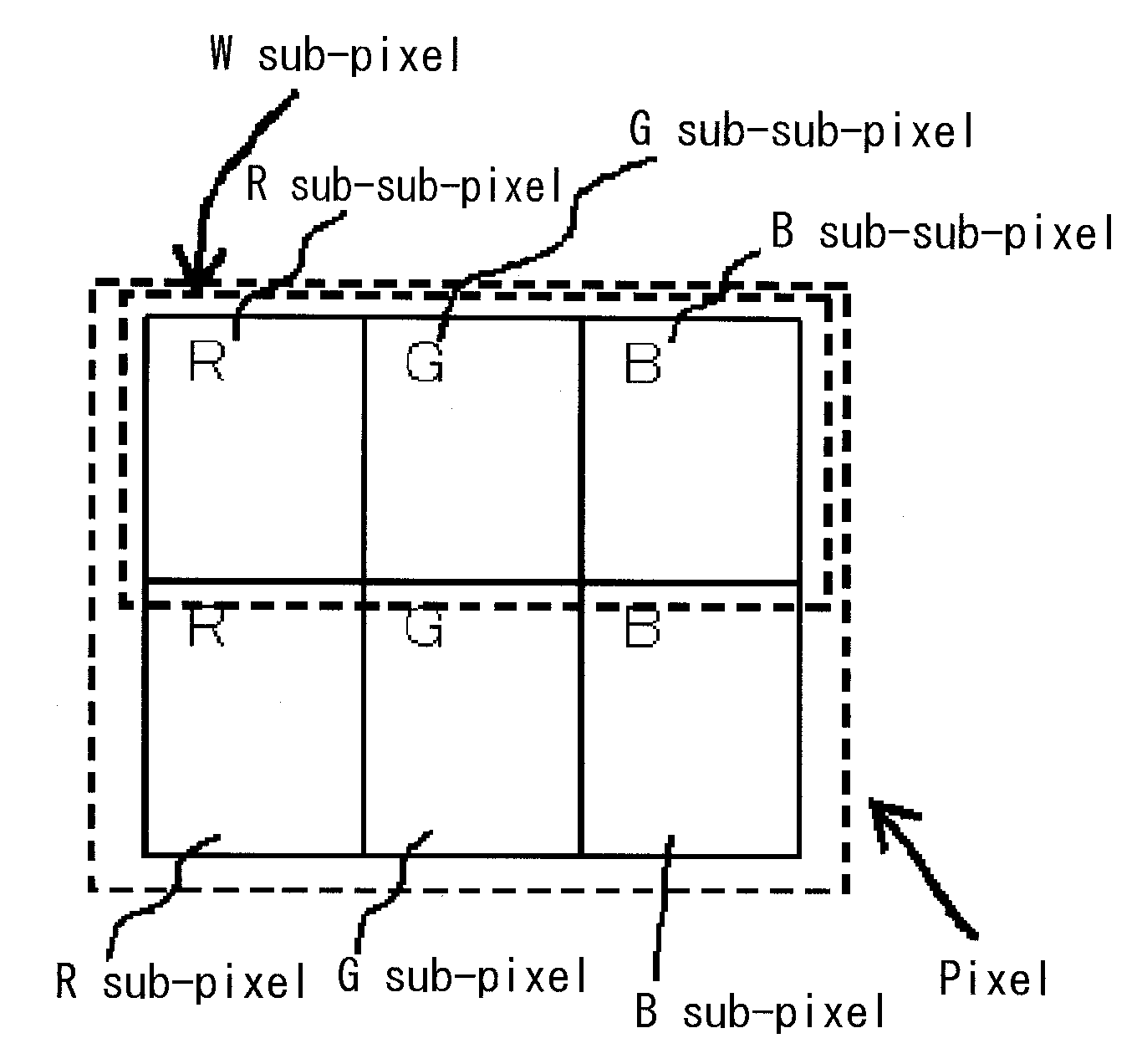
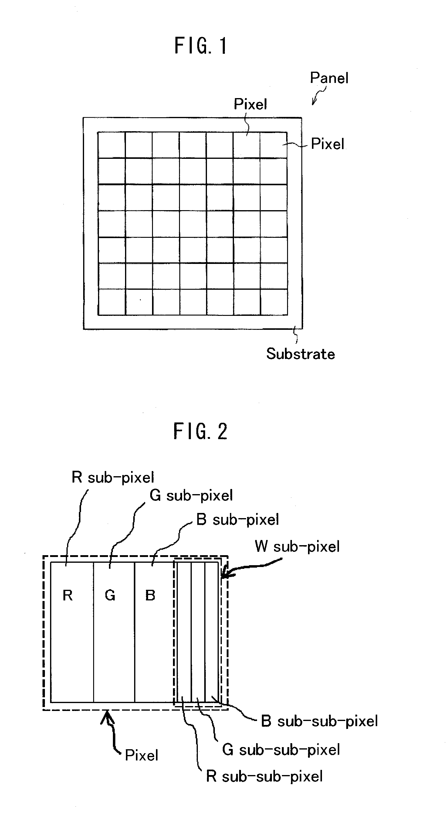
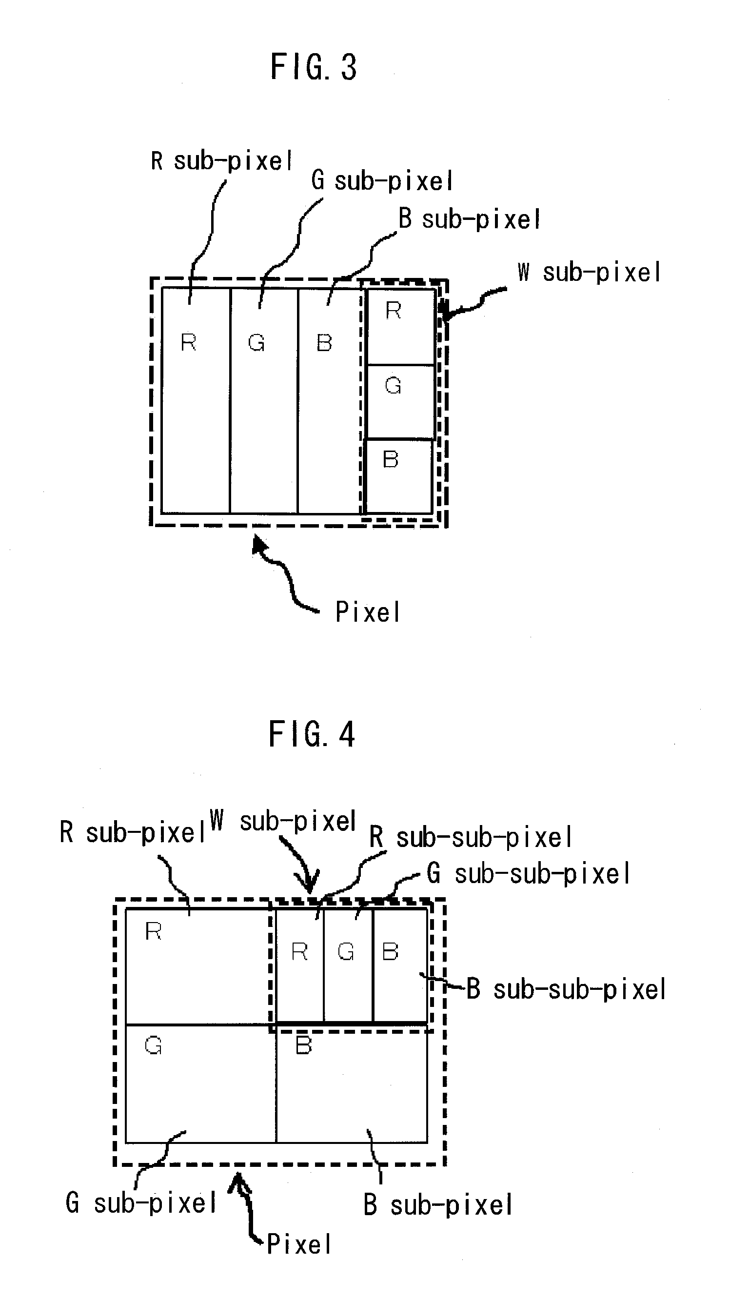
[0218]A method for producing the color display of the invention having the structure shown in FIG. 6 is described with reference to the drawings. FIG. 10 shows production processes in accordance with a process order.[0219](1) A color filter layer (CF layer 2) is formed on a substrate 1. In this process, corresponding to each sub-pixel unit, CR1, CG1, and CB1 are patterned at an R sub-pixel unit, a G sub-pixel unit, and a B sub-pixel unit, respectively, and CR2, CG2, and CB2 are patterned corresponding to each of divided sub-sub-pixel units in the W sub-pixel unit. As a method for patterning, any of a photolithography method using a photosensitive color resist and an ink jet method applying a color resist may be used.[0220](2) A transparent electrode 4 (formed of ITO, IZO, or the like) is formed electrically separately for each sub-pixel on the upper surface of the CF layer 2. The transparent electrode 4 may be patterned by a film forming method using a shadow mask or a photolithogra...
example 2
[0226]A method for producing a color display of the invention having the structure shown in FIG. 7 is described with reference to the drawings. FIG. 11 shows production processes in accordance with a process order.[0227](1) The formation of a color filter CF layer 12 on a substrate 11 is conducted in a similar manner to that in the formation of the CF layer 2 in Example 1.[0228](2) A layer that partially transmits light and partially reflects light 13 is formed on the upper surface of the CF layer 12. The layer that partially transmits light and partially reflects light 13 may be any of metal thin layers (Al, Ag, and the like) and a Distribution Bragg Reflection film (DBR) in which transparent thin layers having a different refractive index are laminated.[0229](3) An optical path length-adjusting layer 17 whose thickness is different according to R, G, and B is formed according to the patterning of the CF layer 12 on the upper surface of the layer that partially transmits light and ...
example 3
[0234]A method for producing a color display of the invention having the structure shown in FIG. 8 is described with reference to the drawings. FIG. 12 shows production processes in accordance with a process order. Examples 1 and 2 are bottom emission types in which an emitted light is taken out from the substrate side. In contrast, Example 3 relates to an embodiment of a top emission type in which the order of disposing the transparent electrode, the white OLED, and the metal electrode is reversed, and light emission is taken out from the upper surface.[0235](1) On a substrate 21, a light-reflection electrode 24, a white organic electroluminescence layer 25, and a transparent electrode 26 are disposed in this order, thereby preparing an OLED substrate.[0236](2) Separately, a color filter substrate in which a CF layer 23 is formed on a transparent substrate 29 in a similar manner to that in the formation of the CF layer 2 of process (1) of Example 1 is prepared.[0237](3) The OLED su...
PUM
 Abstract
Description
Claims
Application Information
 - R&D
- Intellectual Property
- Life Sciences
- Materials
- Tech Scout
- Unparalleled Data Quality
- Higher Quality Content
- 60% Fewer Hallucinations
Browse by: Latest US Patents, China's latest patents, Technical Efficacy Thesaurus, Application Domain, Technology Topic, Popular Technical Reports.
© 2025 PatSnap. All rights reserved.Legal|Privacy policy|Modern Slavery Act Transparency Statement|Sitemap|About US| Contact US: help@patsnap.com


