
Pixel circuit

a pixel circuit and photo sensor technology, applied in the field of solid-state photo sensors, can solve problems such as noise introduction, and achieve the effect of reducing the effective parasitic capacitan

Active Publication Date: 2010-03-04
CSEM CENT SUISSE DELECTRONIQUE & DE MICROTECHNIQUE SA RECH & DEV
View PDF1 Cites 19 Cited by
  • Summary
  • Abstract
  • Description
  • Claims
  • Application Information

AI Technical Summary

Benefits of technology

[0030]The present invention further discloses a method of operating the pixel circuit with a select switch control signal. In embodiments of the invention, the method may for example include the following procedures: configuring, by a first value of the select signal, the select switch, as an open switch to isolate the pixel circuit from the corresponding at least one pixel signal line; configuring, by a second value of the select signal, the select switch as a cascode transistor to connect the pixel output signal to the corresponding at least one signal line; and providing reduced effective parasitic capacitance between the corresponding sense node and signal line for a range of output voltages of the amplifier including the range corresponding to low light intensities, whilst the pixel circuit is isolated from and whilst the pixel output signal is connected to the corresponding at least one signal line.

Problems solved by technology

Downstream circuitry used for signal conditioning such as CDS, amplification and buffering introduces noise of various natures.

Method used


Image

  • Pixel circuit
  • Pixel circuit
  • Pixel circuit

Examples


Embodiment Construction

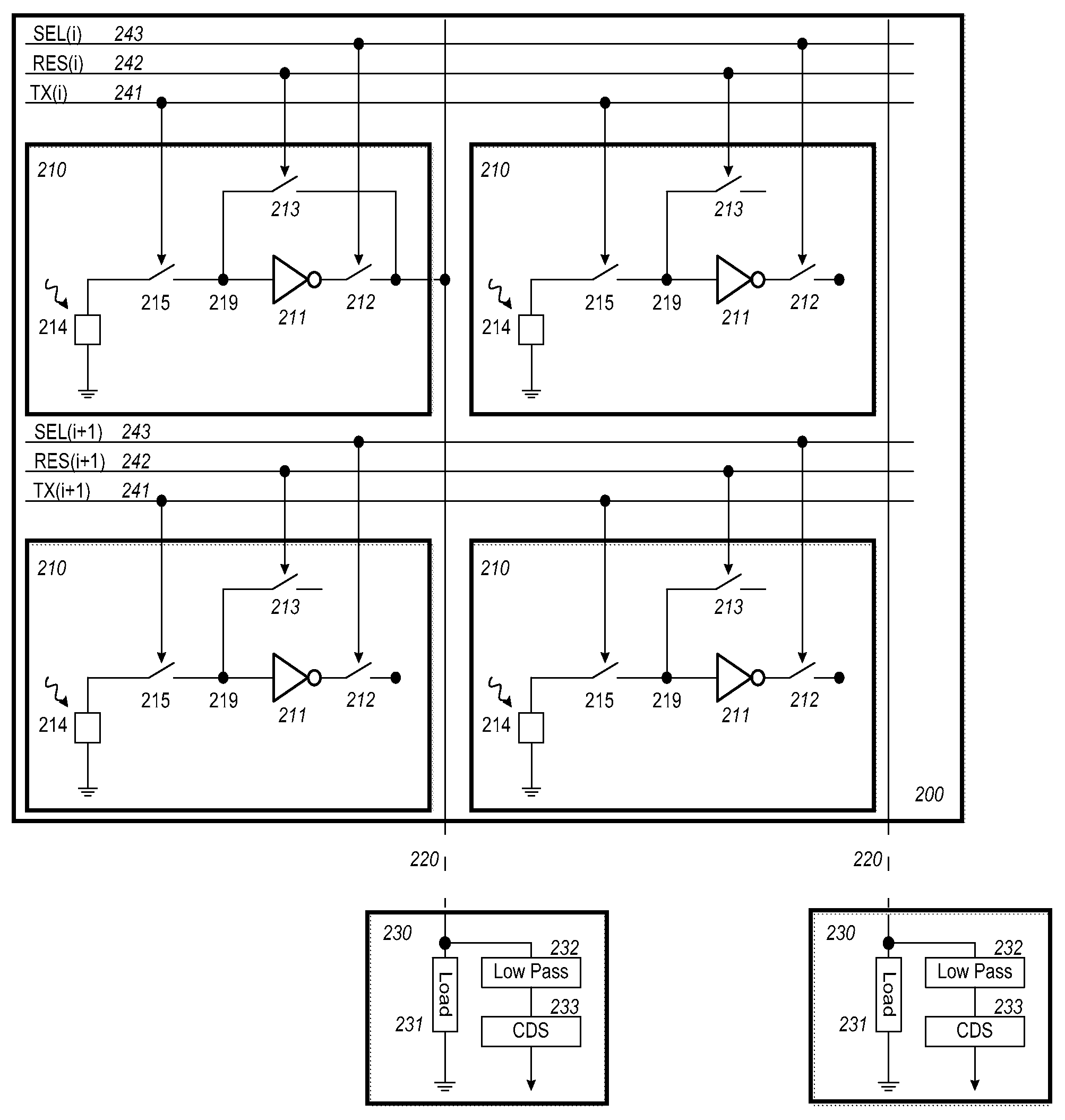
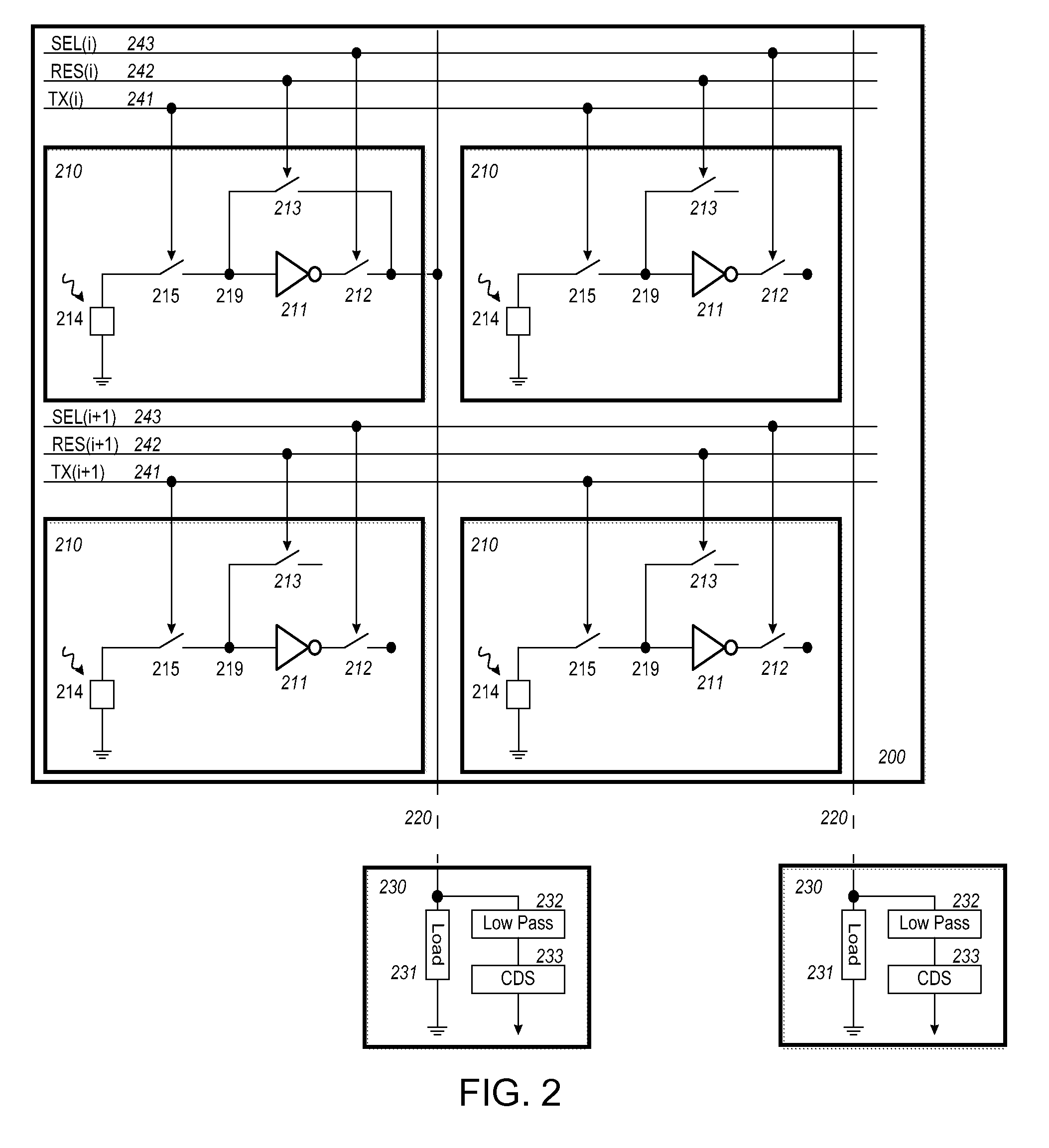
[0022]The present invention refers, inter alia, to pixel circuits. The pixel circuit according to embodiments of the invention may include a photo-sensitive device having charge storage capability connected to a sense node. The pixel circuit may further include an inverting amplifier which is able to amplify a voltage from the sense node to a voltage on an output node of the amplifier, when being operated in open-loop configuration; and a reset switch being able to temporarily establish negative feedback by connecting the input and output nodes of the inverting amplifier and thus to reset the inverting amplifier to an operating point providing high open loop gain. Moreover, the pixel circuit may include a low-pass filter at the output node of the inverting amplifier for the limitation of the signal frequencies passing to the readout node to those frequencies that contain useful signal information.

[0023]In embodiments, the photo-sensitive device may for example be connected to the se...


PUM


Abstract

The present invention refers, inter alia, to pixel circuits. The pixel circuit according to embodiments of the invention may include a photo-sensitive device having charge storage capability connected to a sense node. The pixel circuit may further include an inverting amplifier which is able to amplify a voltage from the sense node to a voltage on an output node of the amplifier, when being operated in open-loop configuration; and a reset switch being able to connect the input and output nodes of the inverting amplifier and thus to reset the inverting amplifier to an operating point providing high open loop gain by temporarily establishing negative feedback. Moreover, the pixel circuit may include a low-pass filter at the output node of the inverting amplifier for limiting the signal frequencies passing to the readout node to those frequencies that contain useful signal information. Additional and alternative embodiments are specified and claimed.

Description

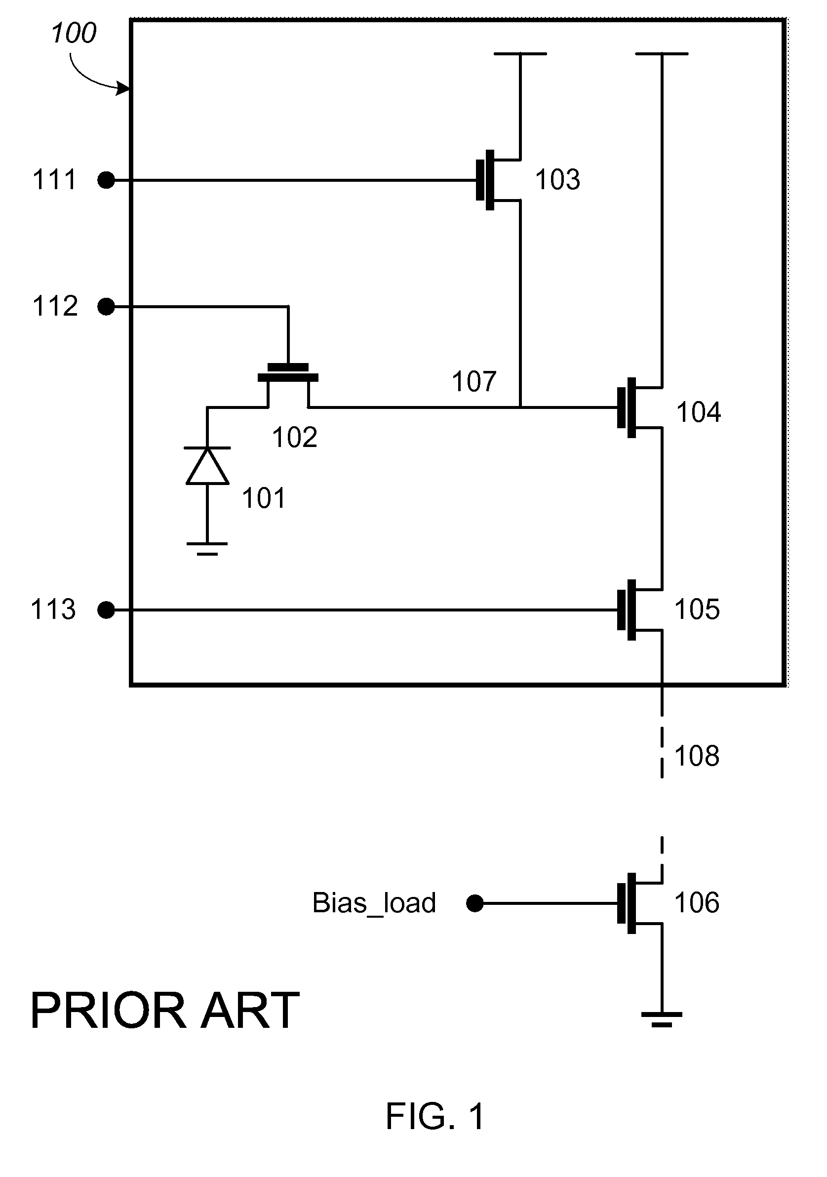
CROSS-REFERENCE TO RELATED APPLICATIONS[0001]The present invention claims priority from EP patent application 08 163 384.4 filed on Sep. 1, 2008, the application which is incorporated herein by reference in its entirety.FIELD OF THE INVENTION[0002]The present invention relates to solid-state photo sensors and more specifically, to solid-state image sensor enabling one-dimensional and two-dimensional imaging.DESCRIPTION OF THE FIGURES[0003]These and further features and advantages of the invention will become more clearly understood in the light of the ensuing description of some embodiments thereof, given by way of example only, with reference to the accompanying figures, wherein:[0004]FIG. 1 is a schematic illustration of an active pixel sensor array according to the prior art;[0005]FIG. 2 is a schematic illustration of a section of an electronic circuit of a sensor array according to an embodiment of the invention;[0006]FIG. 3 is a schematic illustration of an imaging circuit acco...

Claims


Application Information

Patent Timeline
Patent Type & Authority Applications(United States)
IPC IPC(8): H03F3/08H03K17/78H04N25/65
CPCH04N5/35509H04N5/363H04N5/357H04N25/571H04N25/65H04N25/616H04N25/60
Inventor LOTTO, CHRISTIANSEITZ, PETER
Owner CSEM CENT SUISSE DELECTRONIQUE & DE MICROTECHNIQUE SA RECH & DEV
Learn More