Reaction apparatus having multiple adjustable exhaust ports

a technology of reaction apparatus and exhaust port, which is applied in the direction of liquid surface applicators, coatings, metal material coating processes, etc., can solve the problems of reducing the probability of an even deposition across the entire surface of the wafer, reducing the probability of an even deposition, and reducing the probability of uniform deposition. , the effect of reducing the amount of receiving areas

Active Publication Date: 2009-04-30
ASM IP HLDG BV
View PDF50 Cites 17 Cited by
  • Summary
  • Abstract
  • Description
  • Claims
  • Application Information

AI Technical Summary

Benefits of technology

[0008]A need therefore exists to allow a user to control or modify the profile of the gas flow in the reaction chamber to provide substantially uniform distribution of reactant gases across the entire surface of a wafer and reduce the amount of areas receiving a reduced amount or lack of reactant gases. In one aspect of the present invention, a reaction apparatus for use in a semiconductor fabrication apparatus is provided. The reaction apparatus includes a reaction chamber having a first distal end and a second distal end. The reaction apparatus further includes an inlet manifold operatively connected to the first distal end of the reaction chamber. The inlet manifold is configured to introduce reactant gases into the reaction chamber. The reaction apparatus also includes an outlet manifold operatively connected to the second distal end of the reaction chamber. The outlet manifold includes at least two outlet ports from which the gases can exit the reaction chamber. The reaction chamber, inlet manifold and outlet manifold define a flow pattern through the reaction chamber. Each of the outlet ports configured to provide an adjustable flow rate therethrough.

Problems solved by technology

With conventional reaction chambers, the flow pattern within the reaction chamber may develop turbulence along the walls or corners of the reaction chamber.
The flow turbulence can reduce or eliminate the amount of reactant gases at localized areas within the reaction chamber, which is particularly problematic in the areas adjacent to, or above, the exposed surface of the workpiece being processed.
Any type of flow of reactant gases within the reaction chamber that would cause reduced or lack of reactant gases flowing across areas of a wafer reduce the likelihood of an even deposition across the entire surface of the wafer.
Recirculation caused by turbulence can affect not only the uniformity of the deposition but can also create contamination problems.

Method used


Image

  • Reaction apparatus having multiple adjustable exhaust ports
  • Reaction apparatus having multiple adjustable exhaust ports
  • Reaction apparatus having multiple adjustable exhaust ports

Examples


Embodiment Construction

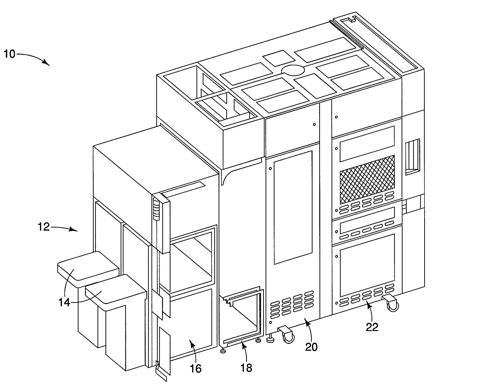
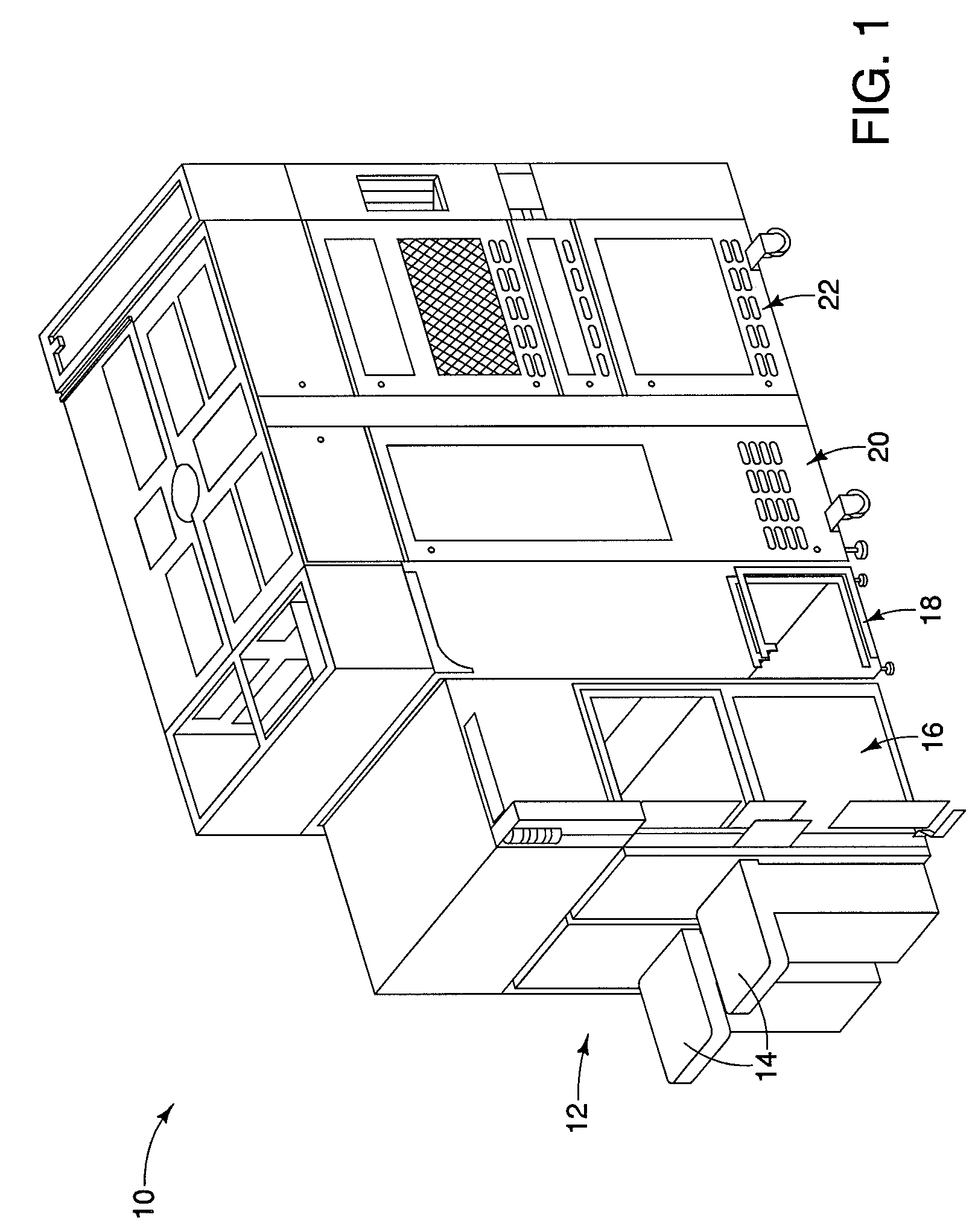
[0021]Referring to FIG. 1, an exemplary embodiment of a semiconductor fabrication apparatus 10 is shown. An example of a suitable commercially available semiconductor fabrication apparatus 10 is the Epsilon® series of tools provided by ASM America, Inc. of Phoenix, Ariz. The semiconductor fabrication apparatus 10 is configured to deposit a thin film, or layer, of a material onto substrates. In an embodiment, the deposition of the thin film is by way of chemical vapor deposition (“CVD”). However, it should be understood by one skilled in the art that the semiconductor fabrication apparatus 10 can be used for semiconductor fabrication using any material deposition process including, but not limited to, atomic layer deposition. The terms “semiconductor wafer,”“substrate,” and / or “wafer” as used herein refers to a substrate as it may exist in any of the various stages of the semiconductor fabrication process.

[0022]In an embodiment, the semiconductor fabrication apparatus 10 includes a f...


PUM

PropertyMeasurementUnit
pressureaaaaaaaaaa
flow rateaaaaaaaaaa
pressureaaaaaaaaaa

Abstract

A reaction apparatus for a semiconductor fabrication apparatus, wherein the reaction apparatus includes at least two adjustable outlet ports for withdrawing reactant gases from the reaction chamber. Adjustment of the flow rate through each of the outlet ports selectively modifies the flow pattern of the reactant gases within the reaction chamber to maintain a desired flow pattern therewithin, such as a substantially uniform flow over the surface of a substrate being processed, and / or minimization of turbulence within the reactor.

Description

FIELD OF THE INVENTION[0001]This invention relates to the manufacture and fabrication of semiconductor devices, and more particularly, this invention relates to methods and structures for controlling the flow pattern within a reaction chamber of a semiconductor processing apparatus.BACKGROUND OF THE INVENTION[0002]In the processing of semiconductor devices, such as transistors, diodes, and integrated circuits, a plurality of such devices are typically fabricated simultaneously on a thin slice of semiconductor material, termed a substrate, wafer, or workpiece. In one example of a semiconductor processing step during manufacture of such semiconductor devices, the wafer or other workpiece is typically transported into a reaction chamber in which a thin film, or layer, of a material is deposited on an exposed surface of the wafer. Once the desired thickness of the layer of semiconductor material has been deposited the surface of the wafer, the wafer may be further processed within the r...

Claims


Application Information

Patent Timeline
Patent Type & Authority Applications(United States)
IPC IPC(8): C23C16/00
CPCC23C16/4412C23C16/455C23C16/45502C23C16/45504C23C16/45563C23C16/458C23C16/4582C23C16/4583C23C16/4584
Inventor AGGARWAL, RAVINDERSTOUTJESDIJK, JEROEN
Owner ASM IP HLDG BV
Why Eureka
Try Eureka