Liquid crystal panel, and liquid crystal display
a liquid crystal display and panel technology, applied in the field of liquid crystal panels and liquid crystal displays, can solve problems such as difficulty in providing neutral displays, and achieve the effect of excellent screen uniformity and high display quality
- Summary
- Abstract
- Description
- Claims
- Application Information
AI Technical Summary
Benefits of technology
Problems solved by technology
Method used
Image
Examples
example 1
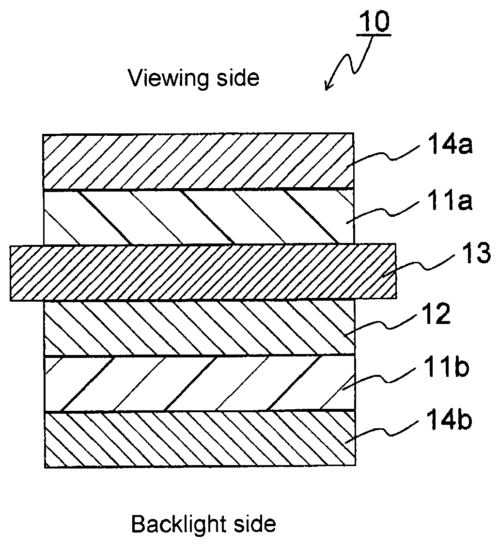
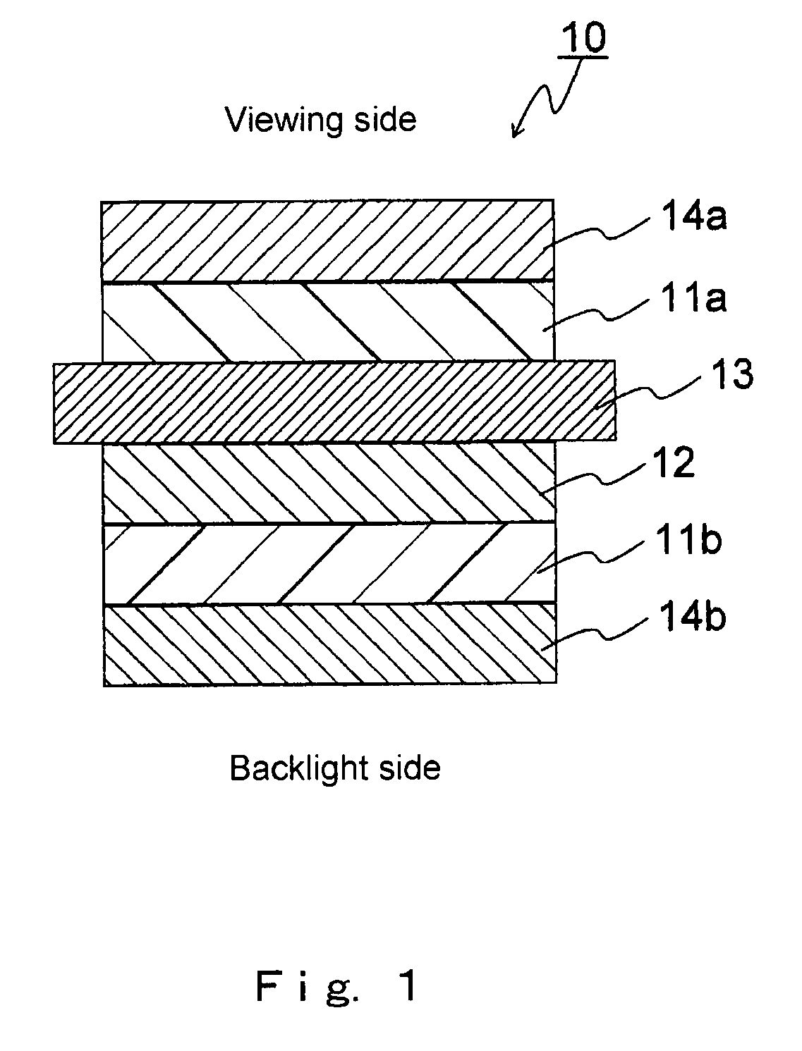
[0201]The optical compensation layer (A) was laminated and adhered to a polarizing plate (“SIG” (trade name) manufactured by NITTO DENKO CORPORATION) via an acrylic pressure-sensitive adhesive having thickness of 20 μm, to thereby prepare a polarizing plate (A) having a compensation layer. At this time, these members were laminated so that the direction of slow axis of the optical compensation layer (A) and the direction of absorption axis of the polarizing plate are orthogonal to each other. The polarizing plate (A) having a compensation layer was prepared in duplicate.
[0202]On the other hand, either one of the two polarizing plates (A) having a compensation layer prepared in the above was selected. The optical compensation layer (B) was laminated and adhered to a surface of optical compensation layer (A) of the polarizing plate (A) having a compensation layer (the surface on the side opposite to the adhesion face of the polarizing plate (A)) via an acrylic pressure-sensitive adhes...
example 2
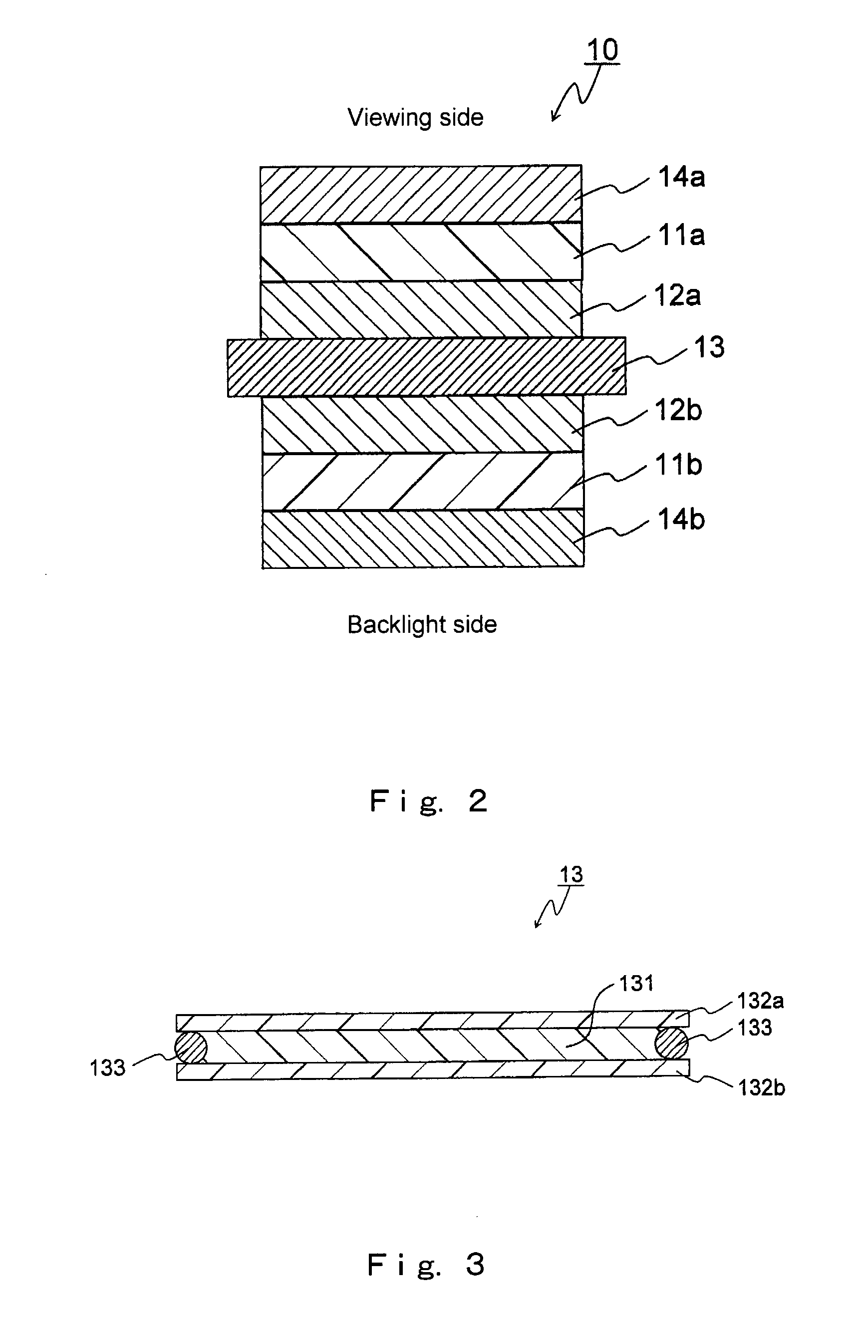
[0208]One polarizing plate (A) having a compensation layer and one polarizing plate (AC) having a compensation layer were fabricated in a similar manner as in Example 1 except that the optical compensation layer (B) used in Example 1 was replaced by the optical compensation layer (C).
[0209]In the polarizing plate (AC) having a compensation layer, a polarizing plate, an optical compensation layer (A) and an optical compensation layer (C) are laminated in this order.
[0210]Then the polarizing plate (A) having a compensation layer was bonded on the viewing side of the liquid crystal cell and the polarizing plate (AC) having a compensation layer was bonded on the opposite viewing side of the liquid crystal cell in a similar manner as in Example 1.
[0211]In this manner, a liquid crystal panel according to Example 2 was fabricated (see Table 2).
[0212]The liquid crystal panel of Example 2 was joined to a backlight unit of the original liquid crystal TV set in a similar manner as in Example 1...
example 3
[0214]The optical compensation layer (D) was laminated and adhered to a polarizing plate (“SIG” (trade name) manufactured by NITTO DENKO CORPORATION) via an acrylic pressure-sensitive adhesive having thickness of 20 μm, to thereby prepare a polarizing plate (D) having a compensation layer. At this time, these members were laminated so that the direction of slow axis of the optical compensation layer (D) and the direction of absorption axis of the polarizing plate are orthogonal to each other. The polarizing plate (D) having a compensation layer was prepared in duplicate.
[0215]On the other hand, either one of the two polarizing plates (D) having a compensation layer prepared in the above was selected. The optical compensation layer (E) was laminated and adhered to a surface of optical compensation layer (D) of the polarizing plate (D) having a compensation layer (the surface on the side opposite to the adhesion face of the polarizing plate (D)) via an acrylic pressure-sensitive adhes...
PUM
| Property | Measurement | Unit |
|---|---|---|
| polar angle | aaaaa | aaaaa |
| thickness | aaaaa | aaaaa |
| polar angle | aaaaa | aaaaa |
Abstract
Description
Claims
Application Information
 - R&D
- Intellectual Property
- Life Sciences
- Materials
- Tech Scout
- Unparalleled Data Quality
- Higher Quality Content
- 60% Fewer Hallucinations
Browse by: Latest US Patents, China's latest patents, Technical Efficacy Thesaurus, Application Domain, Technology Topic, Popular Technical Reports.
© 2025 PatSnap. All rights reserved.Legal|Privacy policy|Modern Slavery Act Transparency Statement|Sitemap|About US| Contact US: help@patsnap.com


