NAND Flash Memory Device And Related Method Thereof
a technology of flash memory and memory device, applied in the field of nand flash memory, can solve the problems of affecting the life of the device, the block could become a “bad” block, and the upper limit on how many times a block can be erased, and achieve the effect of prolonging the lifetim
- Summary
- Abstract
- Description
- Claims
- Application Information
AI Technical Summary
Benefits of technology
Problems solved by technology
Method used
Image
Examples
Embodiment Construction
[0019]The following descriptions are exemplary embodiments only, and are not intended to limit the scope, applicability or configuration of the invention in any way. Rather, the following description provides a convenient illustration for implementing exemplary embodiments of the invention. Various changes to the described embodiments may be made in the function and arrangement of the elements described without departing from the scope of the invention as set forth in the appended claims.
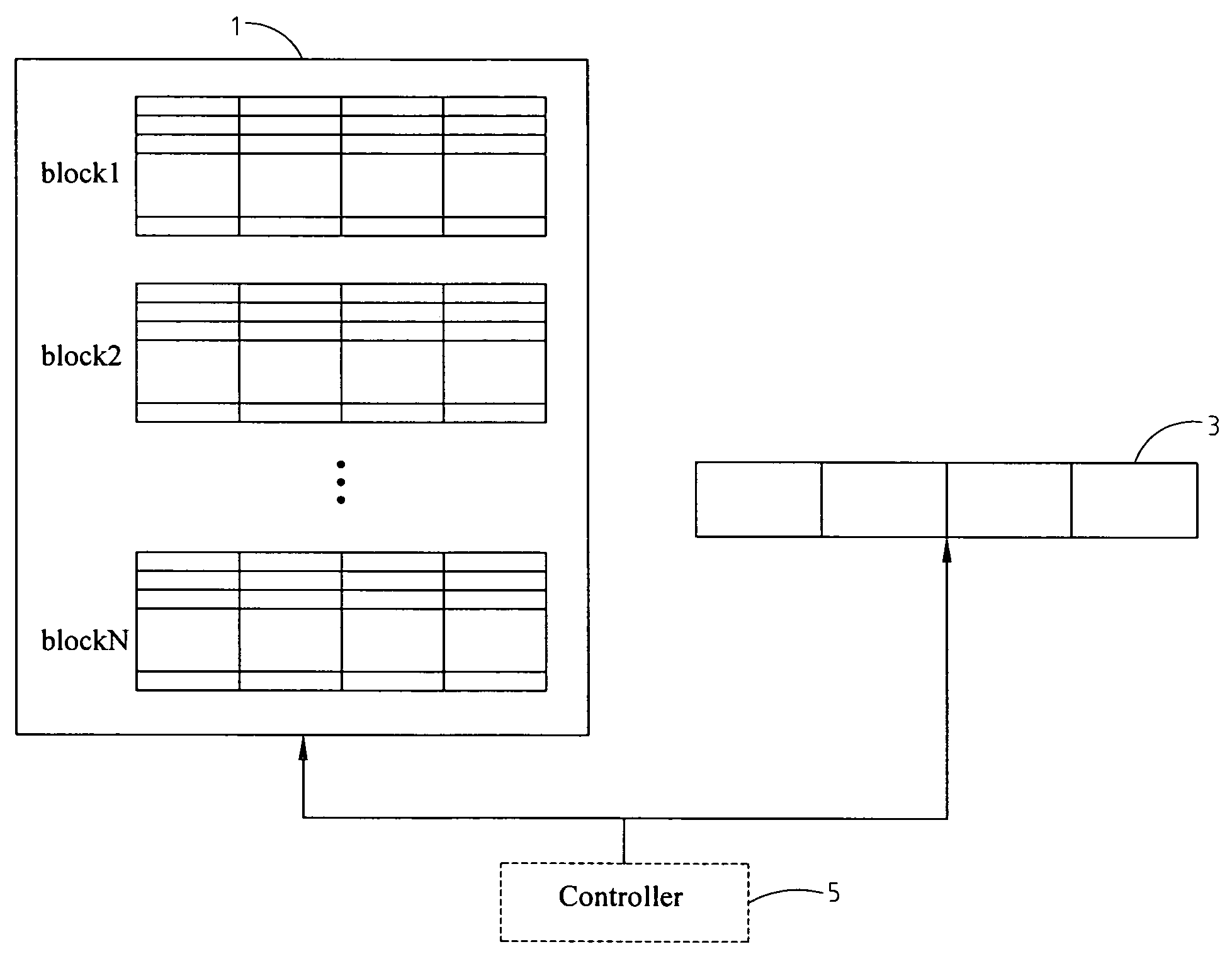
[0020]FIG. 3 is a schematic diagram showing a NAND flash memory device according to an embodiment of the present invention. As illustrated, the NAND flash memory device contains a NAND flash memory 1 which contains a number of blocks (i.e., block1 to blockN). Each block contains a number of pages, each of which in turn contains a number of sectors. In FIG. 3, each page is shown to have 4 sectors. The NAND flash memory device also contains a controller 5 and a mirror data area 3. The mirror data area...
PUM
 Abstract
Description
Claims
Application Information
 - R&D
- Intellectual Property
- Life Sciences
- Materials
- Tech Scout
- Unparalleled Data Quality
- Higher Quality Content
- 60% Fewer Hallucinations
Browse by: Latest US Patents, China's latest patents, Technical Efficacy Thesaurus, Application Domain, Technology Topic, Popular Technical Reports.
© 2025 PatSnap. All rights reserved.Legal|Privacy policy|Modern Slavery Act Transparency Statement|Sitemap|About US| Contact US: help@patsnap.com


