
Pixel structure and liquid crystal display panel

a liquid crystal display panel and pixel structure technology, applied in static indicating devices, instruments, non-linear optics, etc., can solve the problems of color washout, adjustment of the area ratio of the first pixel electrode, and gap between the protruding or slits, so as to avoid the flicker phenomenon of the frame, easy to adjust the area ratio of the sub-pixel, and the effect of avoiding the flicker phenomenon

Active Publication Date: 2008-07-03
NYTELL SOFTWARE LLC
View PDF7 Cites 20 Cited by
  • Summary
  • Abstract
  • Description
  • Claims
  • Application Information

AI Technical Summary

Benefits of technology

[0013]According to the present invention is directed to a pixel structure, a liquid crystal display panel using the pixel structure can eliminate the problem of color shift, make it easy to adjust the area ratio of sub-pixels, and avoid the flicker phenomenon of frame and the loss of aperture ratio.
[0014]The present invention is directed to a liquid crystal display panel capable of eliminating the problem of color shift, easy to adjust the area ratio of sub-pixels and preventing the flicker phenomenon of frame and the loss of aperture ratio.
[0032]The first sub-pixel and the second sub-pixel are formed in a single pixel structure, and the voltage applied to the second sub-pixel is different from the voltage applied to the first sub-pixel by utilizing the capacitance coupling effect between the coupling electrode and the data line. In such way, different electric fields are generated in a single pixel structure to make the liquid crystal molecules alignment along different directions in the single pixel structure. Therefore, the color shift of image can be alleviated.
[0033]Moreover, because the coupling electrode is disposed over the data line, the problem of the loss of aperture ratio due to the assembly shift during the fabrication of the liquid crystal display panel can be effectively prevented. Furthermore, the area ratio of the first sub-pixel to the second sub-pixel in the pixel structure can be easily adjusted and the flicker phenomenon of frame is eliminated.

Problems solved by technology

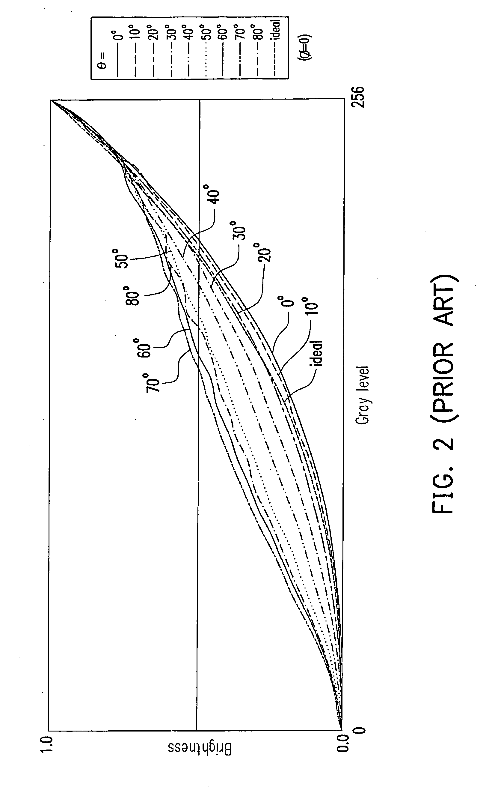
Although the MVA TFT-LCD or a horizontal alignment TFT-LCD can achieve the purpose of the wide viewing angle, users still encounter color washout when viewing an image thereon from different viewing angles.
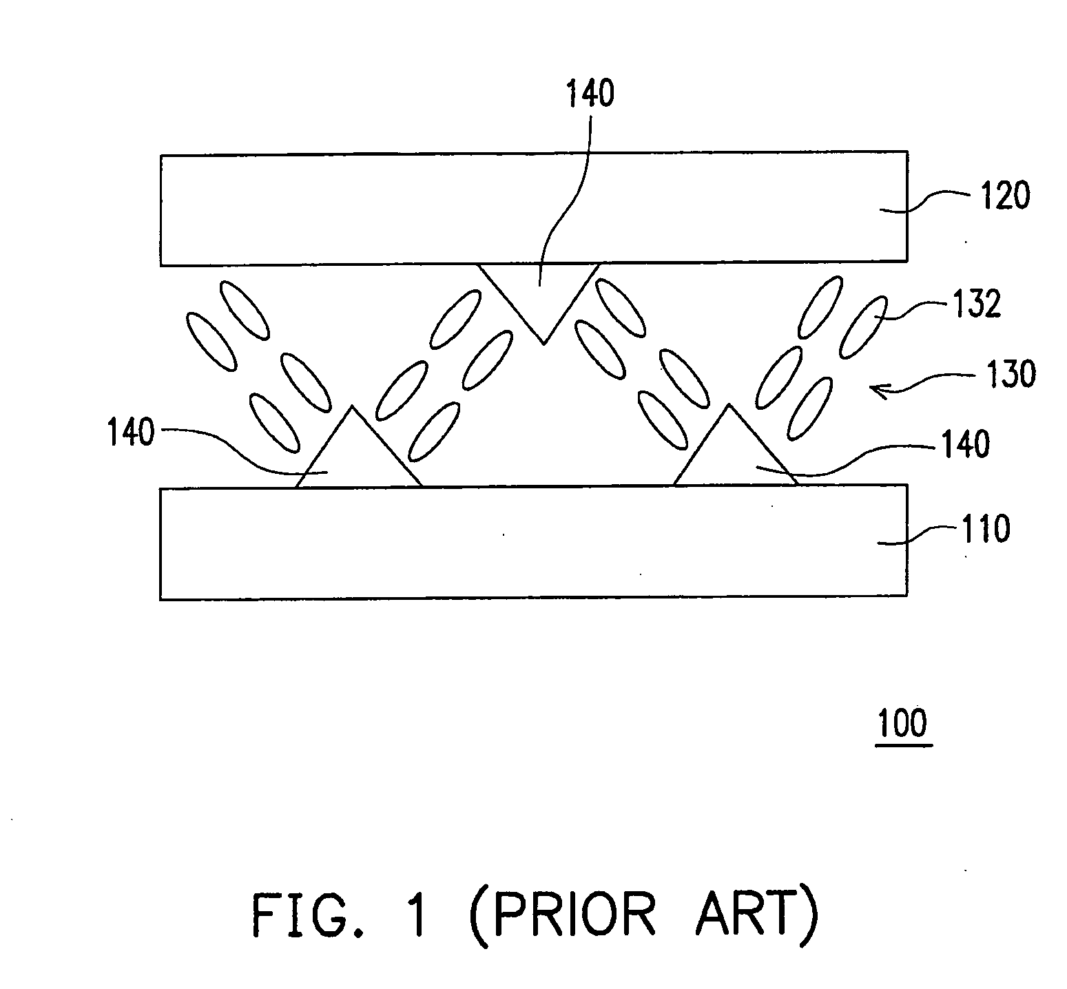
However, complying with the optimistic response time and the transmittance of various panels with different scales and resolutions, the gap between the protrusions or slits is limited, and the adjustment for the area ratio of the first pixel electrode 190a to the second electrode 190b is accordingly restricted.

Method used


Image

  • Pixel structure and liquid crystal display panel
  • Pixel structure and liquid crystal display panel
  • Pixel structure and liquid crystal display panel

Examples


Embodiment Construction

[0051]Reference will now be made in detail to the preferred present embodiments of the invention, examples of which are illustrated in the accompanying drawings. Wherever possible, the same reference numbers are used in the drawings and the description is referred to the same or like parts.

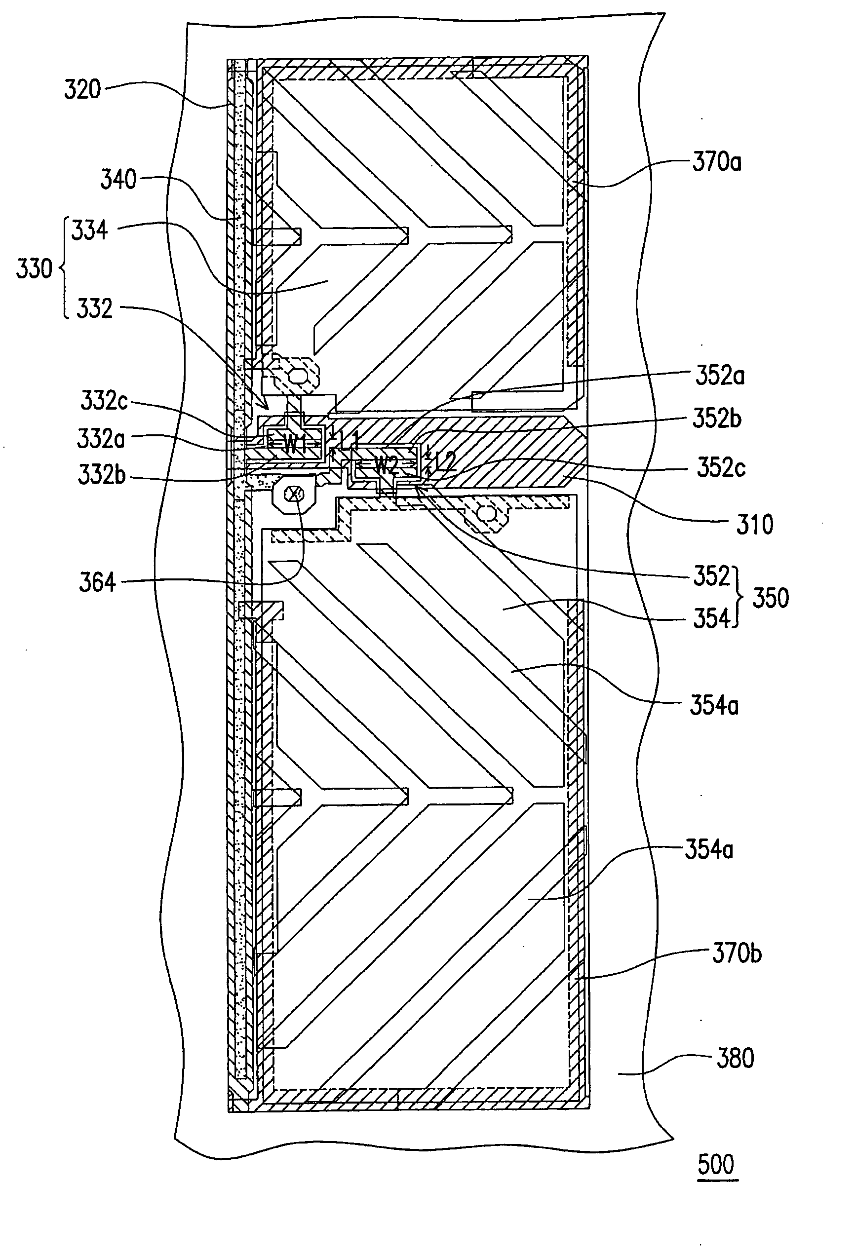
[0052]FIG. 5A is a schematic, top view of a pixel structure according to an embodiment of the present invention. Referring to FIG. 5A, the pixel structure 300 includes a scan line 310, a data line 320, a first sub-pixel 330, a coupling electrode 340 and a second sub-pixel 350. The first sub-pixel 330 includes a first thin film transistor 332 and a first pixel electrode 334, and the first pixel electrode 334 is electrically connected to the scan line 310 and the data line 320 via the first thin film transistor 332. The coupling electrode 340 is disposed above the data line 340 and electrically insulated from the data line 320. The second sub-pixel 350 includes a second thin film transistor 352 and ...


PUM


Abstract

A pixel structure including a scan line, a data line, a first sub-pixel, a coupling electrode and a second sub-pixel is provided. The first sub-pixel includes a first thin film transistor (TFT) and a first pixel electrode, and the first pixel electrode is electrically connected to the scan line and the data line via the first TFT. The coupling electrode is disposed above the data line and electrically insulated from the data line. The second sub-pixel includes a second thin film transistor and a second pixel electrode. The second pixel electrode is electrically connected to the second TFT, and the second TFT is electrically connected to the coupling electrode. When seeing an image from a slant direction, color shift of image can be solved by utilizing the pixel structure. Besides, a liquid crystal display panel having the described pixel structure is also provided.

Description

CROSS-REFERENCE TO RELATED APPLICATION[0001]This application claims the priority benefit of Chinese application serial no. 200610172819.1, filed on Dec. 28, 2006. The entirety of the above-mentioned patent application is hereby incorporated by reference herein and made a part of this specification.BACKGROUND OF THE INVENTION[0002]1. Field of the Invention[0003]The present invention generally relates to a pixel structure and a liquid crystal display panel having the pixel structure, in particular, to a liquid crystal display panel and a pixel structure thereof, which can alleviate color shift of image.[0004]2. Description of Related Art[0005]The thin film transistor liquid crystal display (TFT-LCD) is becoming the mainstream in the display market because of its superior characteristics, such as high image quality, high space utilizing efficiency, low power consumption and no radiation etc.. Recently, high contrast ratio, fast response time and wide viewing angle are the major demands...

Claims


Application Information

Patent Timeline
IPC IPC(8): G02F1/133
CPCG02F1/133707G02F2001/134345G02F1/1393G02F1/13624G02F1/134345
Inventor CHANG, MING-HSUANLIU, CHIH-CHUNGCHANG, YUEH-PING
Owner NYTELL SOFTWARE LLC
Learn More