Pixel structure for electroluminescent panel and method of fabricating same
- Summary
- Abstract
- Description
- Claims
- Application Information
AI Technical Summary
Problems solved by technology
Method used
Image
Examples
Embodiment Construction
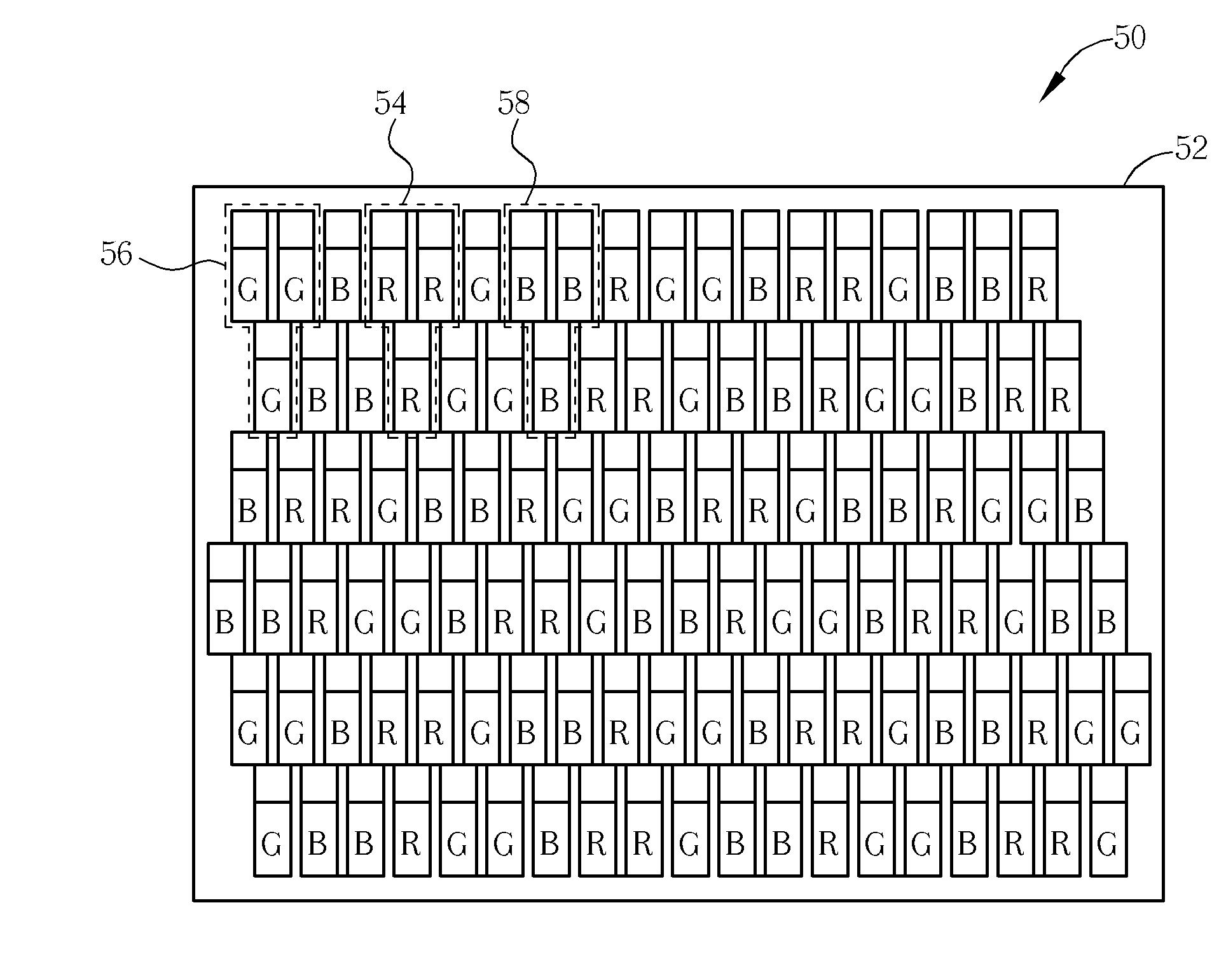
[0022]Please refer to FIG. 5, which is a schematic diagram of a pixel structure for use in an electroluminescent panel according to a preferred embodiment of the present invention. As shown in FIG. 5, the pixel structure 50 comprises a substrate 52, a plurality of first subpixel units 54 disposed on the substrate 52, a plurality of second subpixel units 56 disposed on the substrate 52, and a plurality of third subpixel units 58 disposed on the substrate 52. In the preferred embodiment, the first subpixel units 54, the second subpixel units 56, and the third subpixel units 58 are red, green, and blue subpixel units, respectively, and therefore each first subpixel unit 54 comprises three first subpixels (red subpixels) R arranged in a delta formation, each second subpixel unit 56 comprises three second subpixels (green subpixels) G arranged in a delta formation, and each third subpixel unit 58 comprises three third subpixels (blue subpixels) B arranged in a delta formation.
[0023]In th...
PUM
 Abstract
Description
Claims
Application Information
 - R&D
- Intellectual Property
- Life Sciences
- Materials
- Tech Scout
- Unparalleled Data Quality
- Higher Quality Content
- 60% Fewer Hallucinations
Browse by: Latest US Patents, China's latest patents, Technical Efficacy Thesaurus, Application Domain, Technology Topic, Popular Technical Reports.
© 2025 PatSnap. All rights reserved.Legal|Privacy policy|Modern Slavery Act Transparency Statement|Sitemap|About US| Contact US: help@patsnap.com


