Polishing pad surface shape measuring instrument, method of using polishing pad surface shape measuring instrument, method of measuring apex angle of cone of polishing pad, method of measuring depth of groove of polishing pad, CMP polisher, and method of manufacturing semiconductor device

Active Publication Date: 2006-11-23
NIKON CORP
View PDF4 Cites 14 Cited by
  • Summary
  • Abstract
  • Description
  • Claims
  • Application Information

AI Technical Summary

Benefits of technology

[0012] The present invention was devised in light of the above circumstances; it is an object of the present invention to provide a polishing pad surface shape measuring device which can be disposed inside the main body of a CMP polishing apparatus, and which makes it possible to perform measurements without removing the polishing pad, a method of use of this polishing pad surface shape measuring device, a polishing pad circular-conical vertical angle measurement method, a polishing pad groove depth measurement method, a CMP polishing apparatus equipped with the polishing pad surface shape measuring device, and a semiconductor device manufacturing method using this CMP polishing apparatus.

Problems solved by technology

As semiconductor integrated circuits have become finer and more highly integrated, the steps involved in semiconductor manufacturing processes have increased in number and become more complicated.
As a result, the surface state of a semiconductor device is no longer necessarily flat.
The presence of steps on such surfaces leads to the breakage of wiring by steps, an increase in local resistance values, and the like, thus resulting in loss of wire connections, a drop in current capacity, and the like.
Furthermore, this also leads to a deterioration in the withstand voltage and the occurrence of leaks in insulating films.
Thus, conventionally, there has been no means for observing the surface of the polishing pad inside the CMP apparatus, so that the shape is measured after first temporarily removing the polishing pad from the polishing chamber.
However, removing the polishing pad from the rotating type swinging arm every time that the shape of the polishing pad is to be measured requires the expenditure of considerable effort; consequently, not only is the throughput lowered, but when he polishing pad is again mounted on the rotating platen, the mounted state differs from that prior to the removal of the polishing pad.
As a result, distortion is newly generated, so that the flatness deteriorates, and there may be cases in which the desired polishing cannot be performed.

Method used


Image

  • Polishing pad surface shape measuring instrument, method of using polishing pad surface shape measuring instrument, method of measuring apex angle of cone of polishing pad, method of measuring depth of groove of polishing pad, CMP polisher, and method of manufacturing semiconductor device
  • Polishing pad surface shape measuring instrument, method of using polishing pad surface shape measuring instrument, method of measuring apex angle of cone of polishing pad, method of measuring depth of groove of polishing pad, CMP polisher, and method of manufacturing semiconductor device
  • Polishing pad surface shape measuring instrument, method of using polishing pad surface shape measuring instrument, method of measuring apex angle of cone of polishing pad, method of measuring depth of groove of polishing pad, CMP polisher, and method of manufacturing semiconductor device

Examples


Embodiment Construction

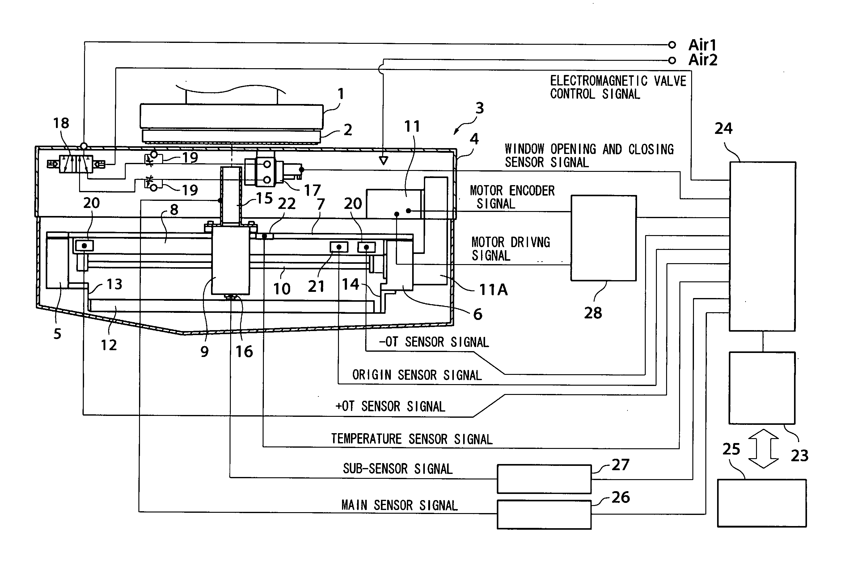
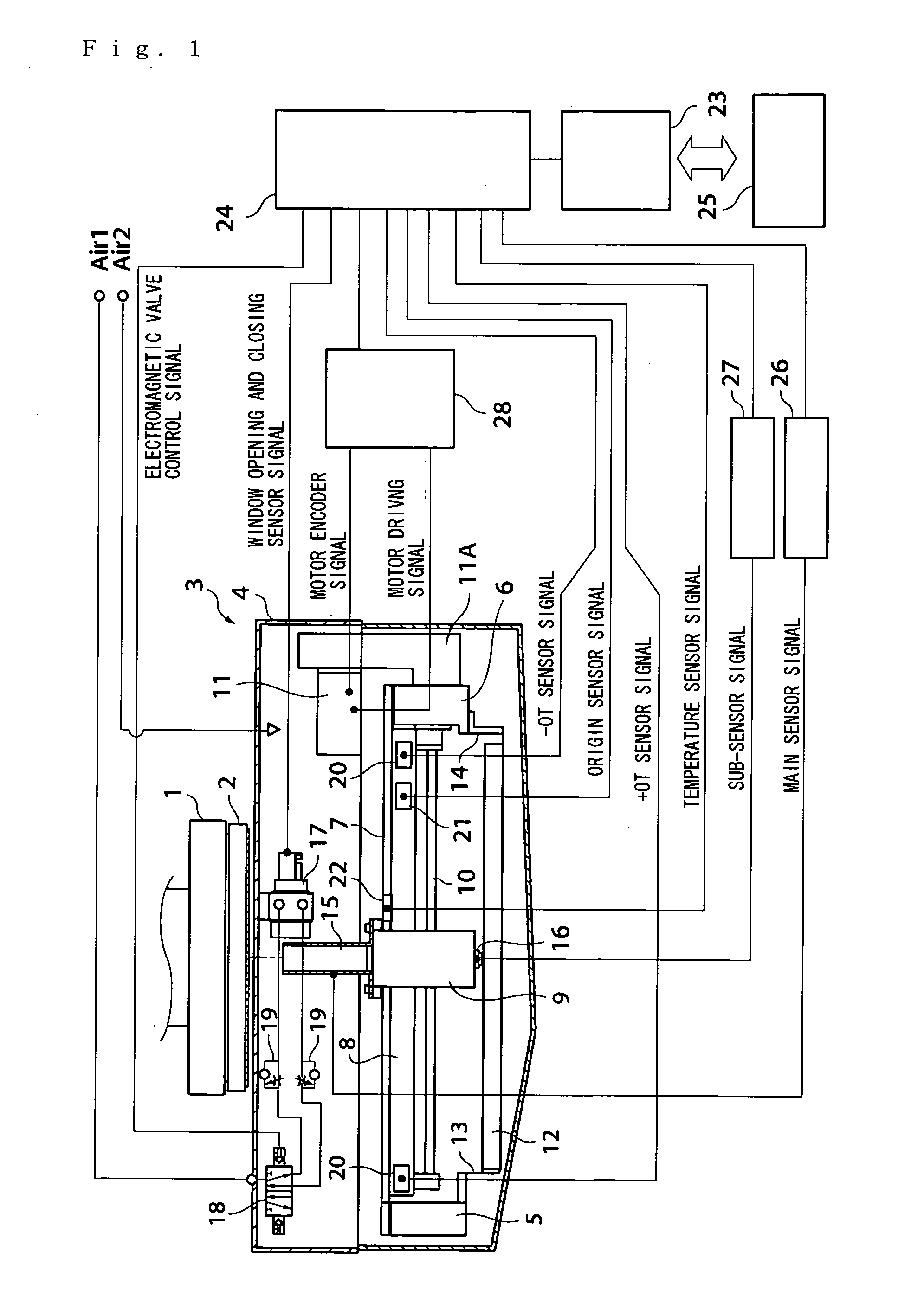
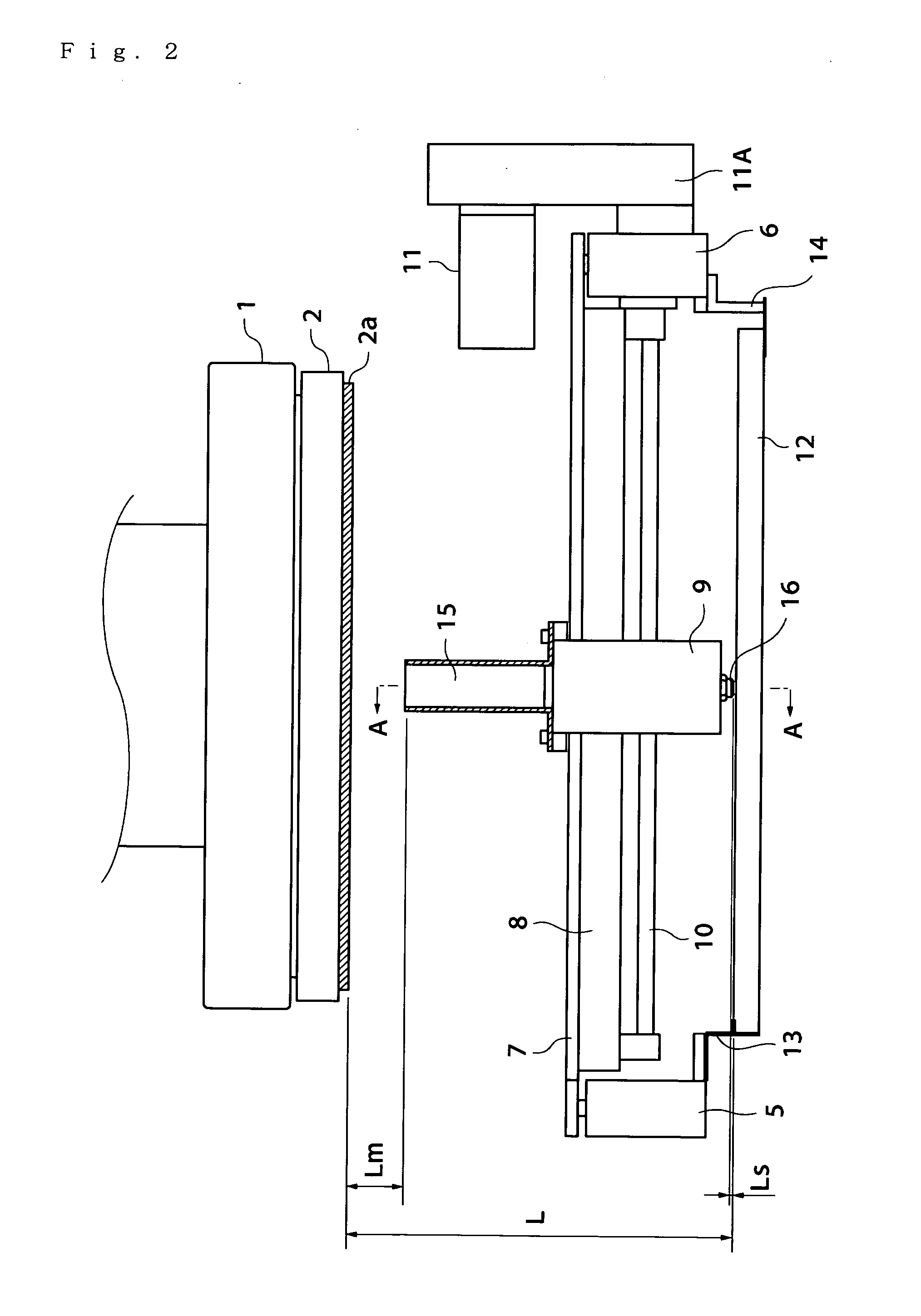
[0073] Working configurations of the present invention will be described below with reference to the figures. FIG. 1 is an overall schematic diagram showing the construction of a polishing pad surface shape measuring device constituting a first example of a working configuration of the present invention. A polishing pad 2 is attached to the polishing head 1 by vacuum suction or the like. The polishing pad 2 is a part in which a polishing cloth called a pad such as a foam polyurethane is pasted to a metal pad plate. The polishing pad 2 is held on the tip end of a rotatable shaft by vacuum suction or the like. The mechanism that performs the rotational holding of this polishing pad is called the polishing head 1. The polishing cloth called a pad generally has lattice-form grooves, so that diffusion of the polishing liquid is promoted during polishing. The groove width is approximately 1 mm, and the depth is also approximately 1 mm.

[0074] The main body part 3 of the polishing pad surf...


PUM

PropertyMeasurementUnit
Angleaaaaaaaaaa
Angleaaaaaaaaaa
Thicknessaaaaaaaaaa

Abstract

The main sensor 15 measures the distance Lm to the surface of the pad 2a, and the sub-sensor 16 measures the distance Ls to the surface of the reference block 12. What is actually taken as the measured value is the value of (Lm+Ls). The reference block 12 is used in order to give a reference position for measuring the surface position of the pad 2a. Accordingly, correct measurements can be performed even if the position of the movable element 9 should fluctuate, for example, as a result of deformation of the guiding and holding plate 7 or guide 8. When the motor 11 is caused to rotate, the ball screw 10 rotates, so that the movable element 9 moves leftward and rightward, and the distance to the pad 2a is measured. From the measured data of this distance, the circular-conical vertical angle, groove depth, thickness, and the like of the pad 2a are determined

Description

TECHNICAL FIELD [0001] The present invention relates to a surface shape measuring device for a polishing pad used in a CMP polishing apparatus or the like, a method of use for this polishing pad surface shape measuring device, a polishing pad circular-conical vertical angle measurement method, a polishing pad groove depth measurement method, a CMP polishing apparatus, and a semiconductor device manufacturing method. BACKGROUND ART [0002] As semiconductor integrated circuits have become finer and more highly integrated, the steps involved in semiconductor manufacturing processes have increased in number and become more complicated. As a result, the surface state of a semiconductor device is no longer necessarily flat. The presence of steps on such surfaces leads to the breakage of wiring by steps, an increase in local resistance values, and the like, thus resulting in loss of wire connections, a drop in current capacity, and the like. Furthermore, this also leads to a deterioration i...

Claims


Application Information

Patent Timeline
IPC IPC(8): C03C15/00H01L21/306B24B49/12B24B49/18B24B53/017H01L21/304
CPCB24B37/26B24B49/18B24B49/12H01L21/304
Inventor TANAKA, TOSHIHISATANAKA, ATSUSHISOMA, TAKESHI
Owner NIKON CORP
Why Eureka
Try Eureka