
Method to form a passivation layer

a technology of passivation layer and passivation layer, which is applied in the direction of electrical equipment, semiconductor devices, instruments, etc., can solve the problems of not being able to produce the desired, time-consuming and/or expensive, and not allowing the use of particular materials

Active Publication Date: 2006-04-13
HEWLETT PACKARD DEV CO LP +1
View PDF19 Cites 102 Cited by
  • Summary
  • Abstract
  • Description
  • Claims
  • Application Information

AI Technical Summary

Problems solved by technology

For example, such techniques may be time-consuming and / or expensive, may not allow for the use of particular materials, and / or may not produce the desired results.

Method used


Image

  • Method to form a passivation layer
  • Method to form a passivation layer
  • Method to form a passivation layer

Examples


Embodiment Construction

[0006] In the following detailed description, numerous specific details are set forth to provide a thorough understanding of claimed subject matter. However, it will be understood by those skilled in the art that claimed subject matter may be practiced without these specific details. In other instances, well-known methods, procedures, components and / or circuits have not been described in detail so as not to obscure claimed subject matter.

[0007] Electronic devices, such as semiconductor devices, display devices, nanotechnology devices, conductive devices, and / or dielectric devices, for example, may be comprised of one or more electronic components. One or more of these electronic components may be comprised of one or more thin films, such as a plurality of thin films, which may additionally be referred to as layers. In this context, the term thin film refers to a material formed to a thickness, such that surface properties of the material may be observed, and these properties may va...


PUM


Abstract

Embodiments of methods, apparatuses, devices, and / or systems for forming a passivation layer are described.

Description

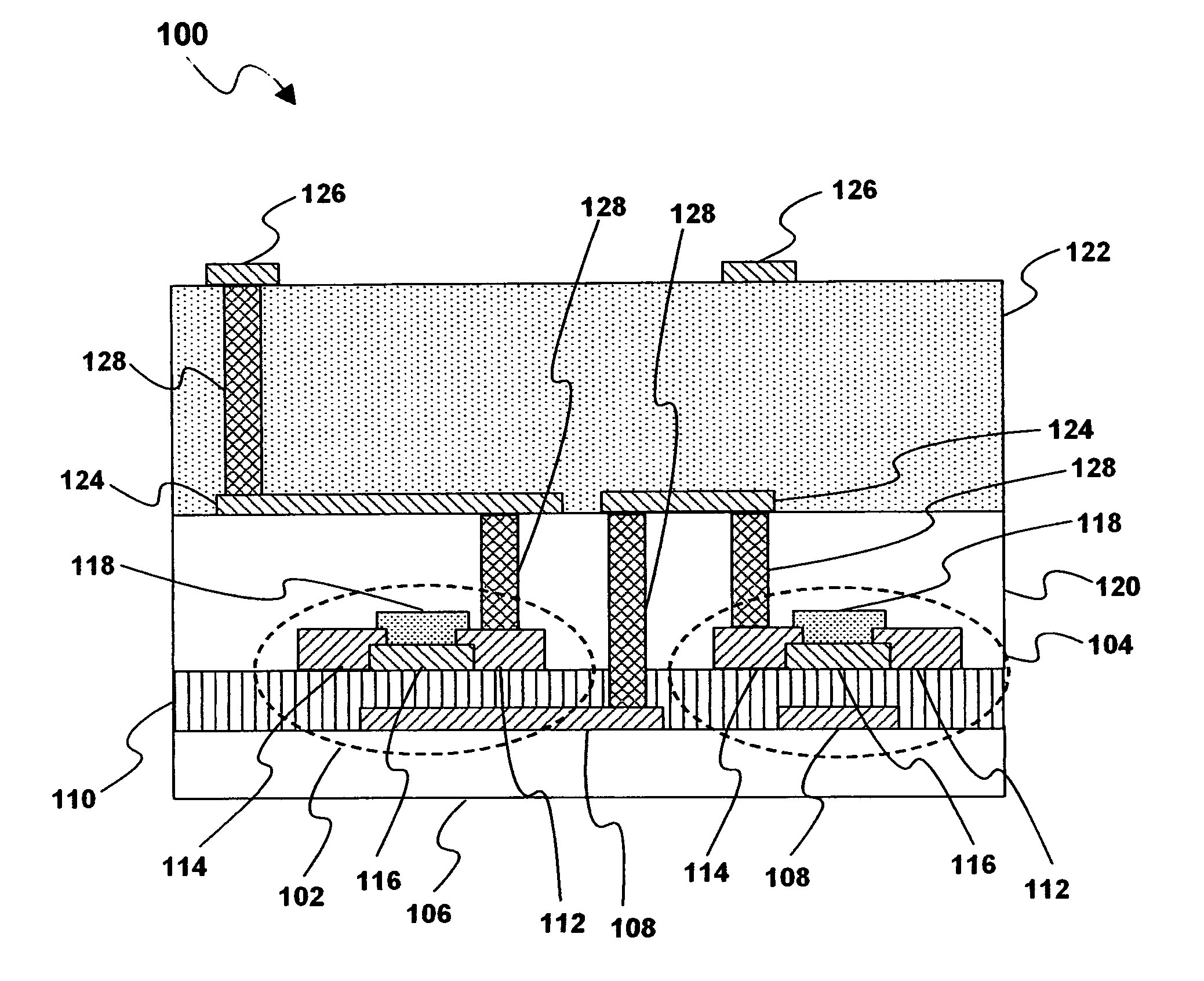
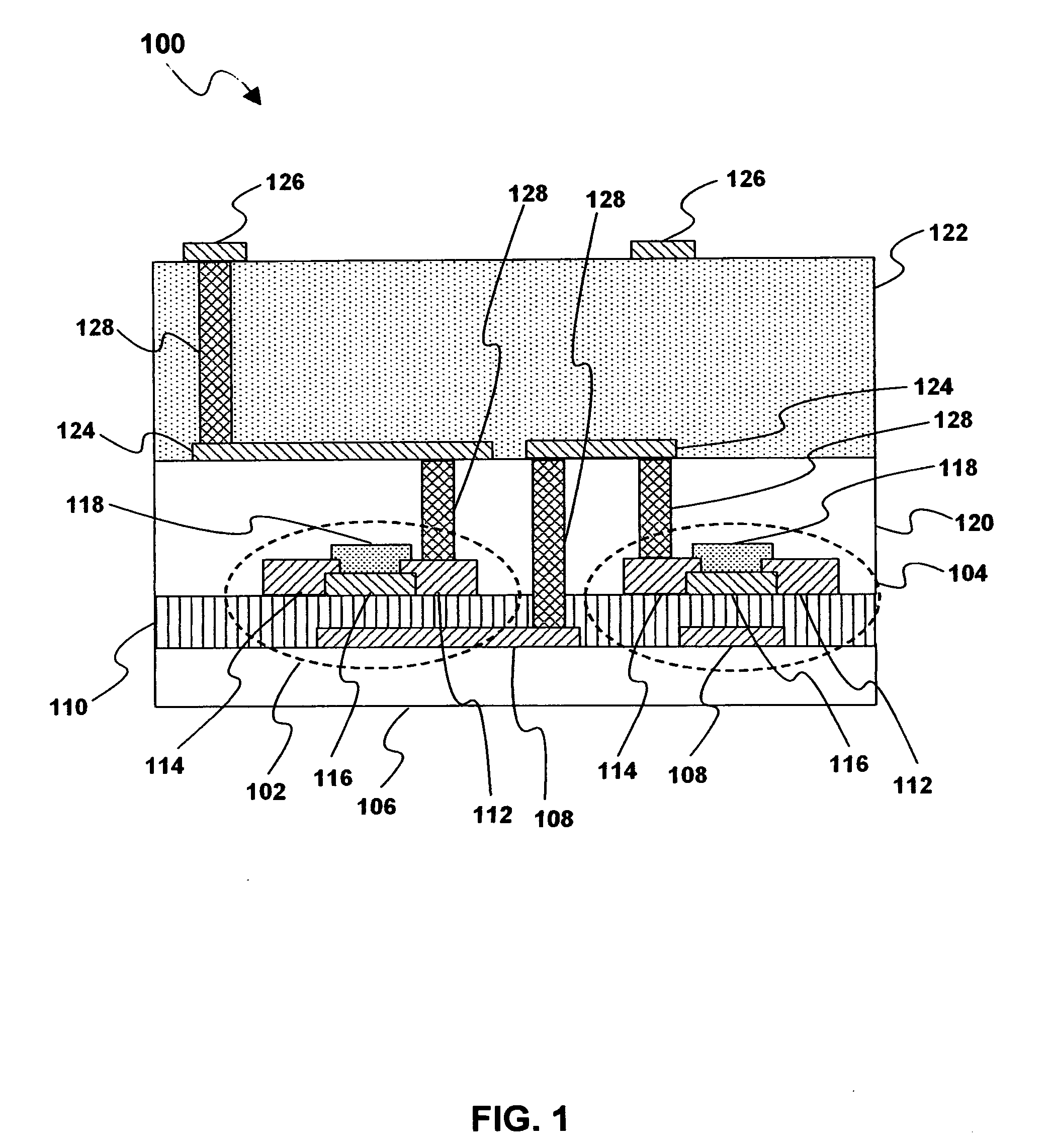
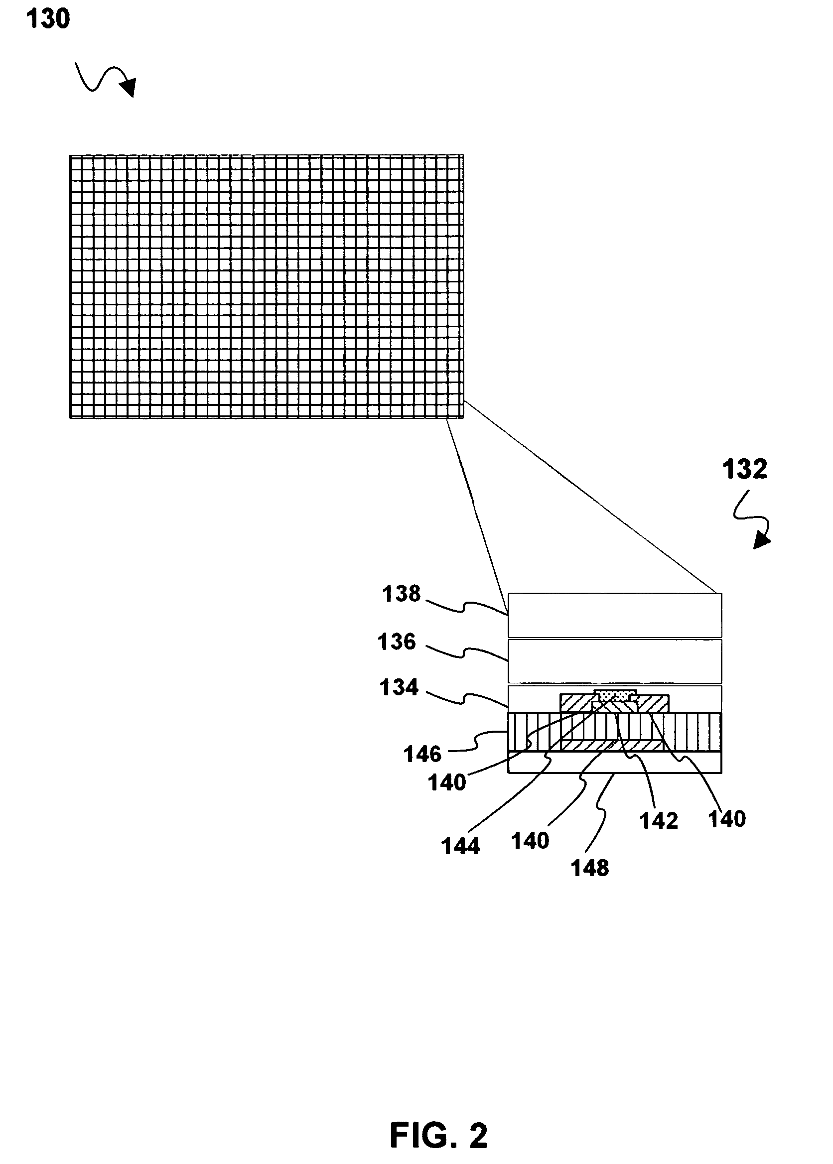
BACKGROUND [0001] Electronic devices, such as integrated circuits, solar cells, and / or electronic displays, for example, may be comprised of one or more electrical components, such as one or more thin film transistors. Thin film transistors may be formed from one or more layers, which may be stacked, for example. In at least one type of electronic device, multiple thin film transistors may be coupled to form circuitry, such as a circuitry comprising a plurality of thin film transistors. When forming circuitry such as this, varying techniques may be utilized to isolate, separate and / or insulate one or more transistors and / or layers from one another, for example. Although particular techniques may vary, one or more techniques may have particular disadvantages. For example, such techniques may be time-consuming and / or expensive, may not allow for the use of particular materials, and / or may not produce the desired results.BRIEF DESCRIPTION OF THE DRAWINGS [0002] Subject matter is partic...

Claims


Application Information

Patent Timeline
Patent Type & Authority Applications(United States)
IPC IPC(8): H01L21/84
CPCH01L29/66969H01L29/7869
Inventor HOFFMAN, RANDYWAGER, JOHNHONG, DAVIDCHIANG, HAI
Owner HEWLETT PACKARD DEV CO LP
Learn More