Method for manufacturing device isolation film of semiconductor device

a technology of isolation film and semiconductor device, which is applied in the direction of semiconductor devices, basic electric elements, electrical equipment, etc., can solve the problems of reducing active region width, deteriorating gap-fill characteristics, and reducing device characteristics and yield, so as to reduce or prevent the phenomenon of heip

Active Publication Date: 2006-02-02
SK HYNIX INC
View PDF15 Cites 32 Cited by
  • Summary
  • Abstract
  • Description
  • Claims
  • Application Information

AI Technical Summary

Benefits of technology

[0015] A method for a method for manufacturing a device isolation film of a semiconductor device is provided, wherein a liner nitride film exposed by removing a liner oxide film in a peripheral region is oxidized using plasma prior to the formation of a device isolation film so that HEIP phenomenon is reduced or prevented, thereby improving semiconductor device characteristics such as a refresh characteristic and a current driving capability.

Problems solved by technology

The HEIP phenomenon increases a stand-by current of a DRAM, which degrades device characteristics and yield.
However, as the thickness of the sidewall oxide film increases, gap-fill characteristics deteriorate and active region width decreases.
The deterioration of gap-fill characteristics and decrease in active region width reduces the current driving capability and threshold voltage of a transistor, and degrades refresh characteristics of the transistor.

Method used


Image

  • Method for manufacturing device isolation film of semiconductor device
  • Method for manufacturing device isolation film of semiconductor device
  • Method for manufacturing device isolation film of semiconductor device

Examples


Embodiment Construction

[0020] Reference will now be made in detail to exemplary embodiments of the present invention. Wherever possible, the same reference numbers will be used throughout the drawings to refer to the same or like parts.

[0021]FIGS. 2a through 2g are cross-sectional diagrams illustrating a method for manufacturing a device isolation film of a semiconductor device in accordance with an embodiment of the present invention.

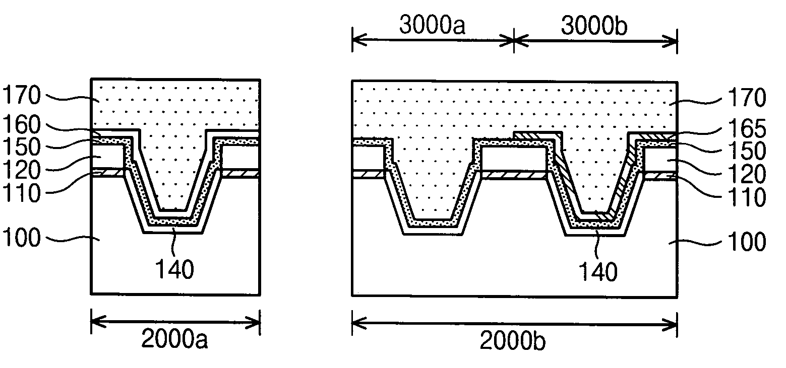
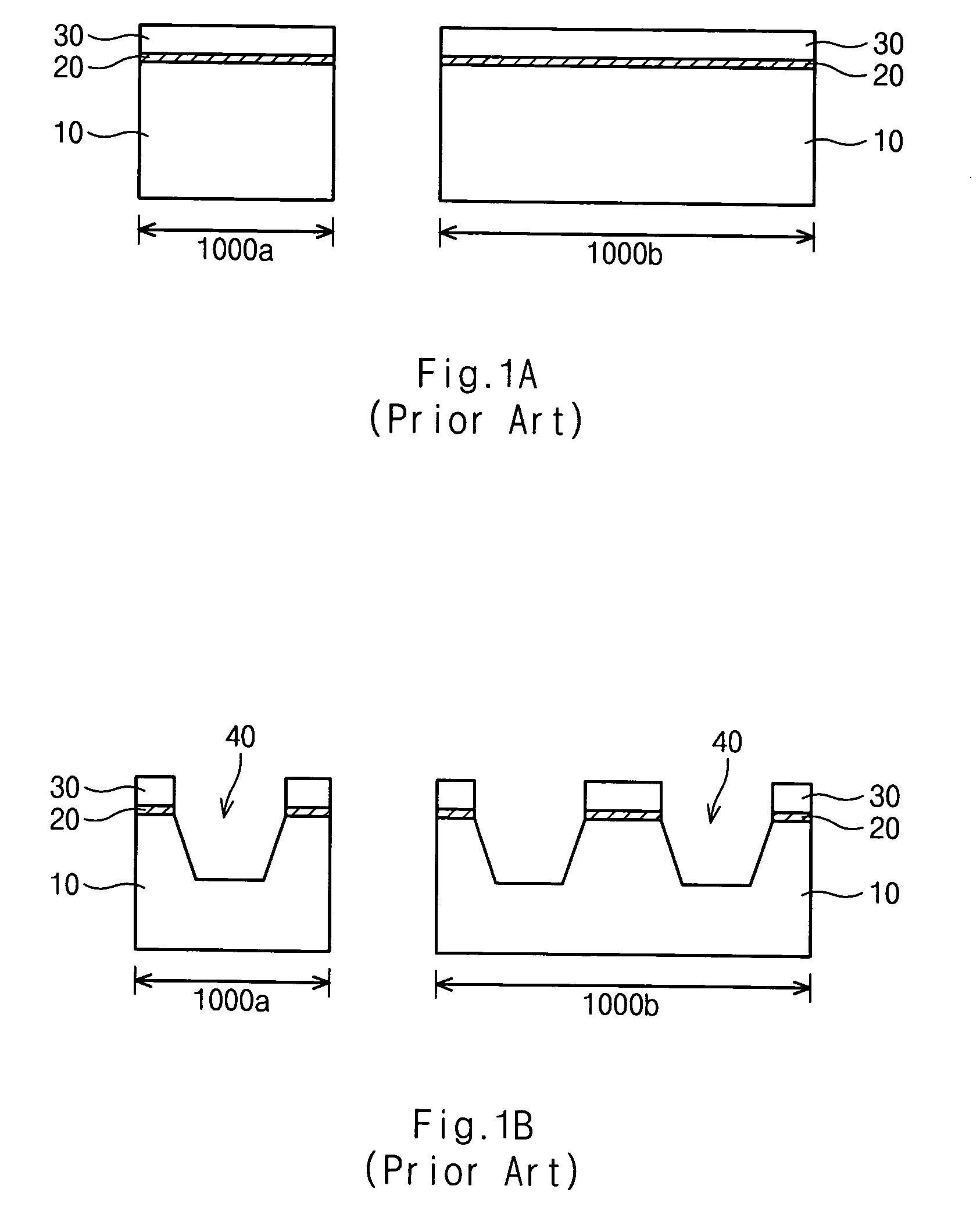
[0022] Referring to FIG. 2a, a pad oxide film 110 and a pad nitride film 120 are sequentially formed on a semiconductor substrate 100. The semiconductor substrate 100 comprises a cell region 2000a and a peripheral region 2000b. The peripheral region 2000b also includes a pMOS region 3000a and an nMOS region 3000b.

[0023] Referring to FIG. 2b, a predetermined region of the pad nitride film 120, the pad oxide film 110 and the semiconductor substrate 100 where a device isolation film is to be formed is etched to form a trench 130.

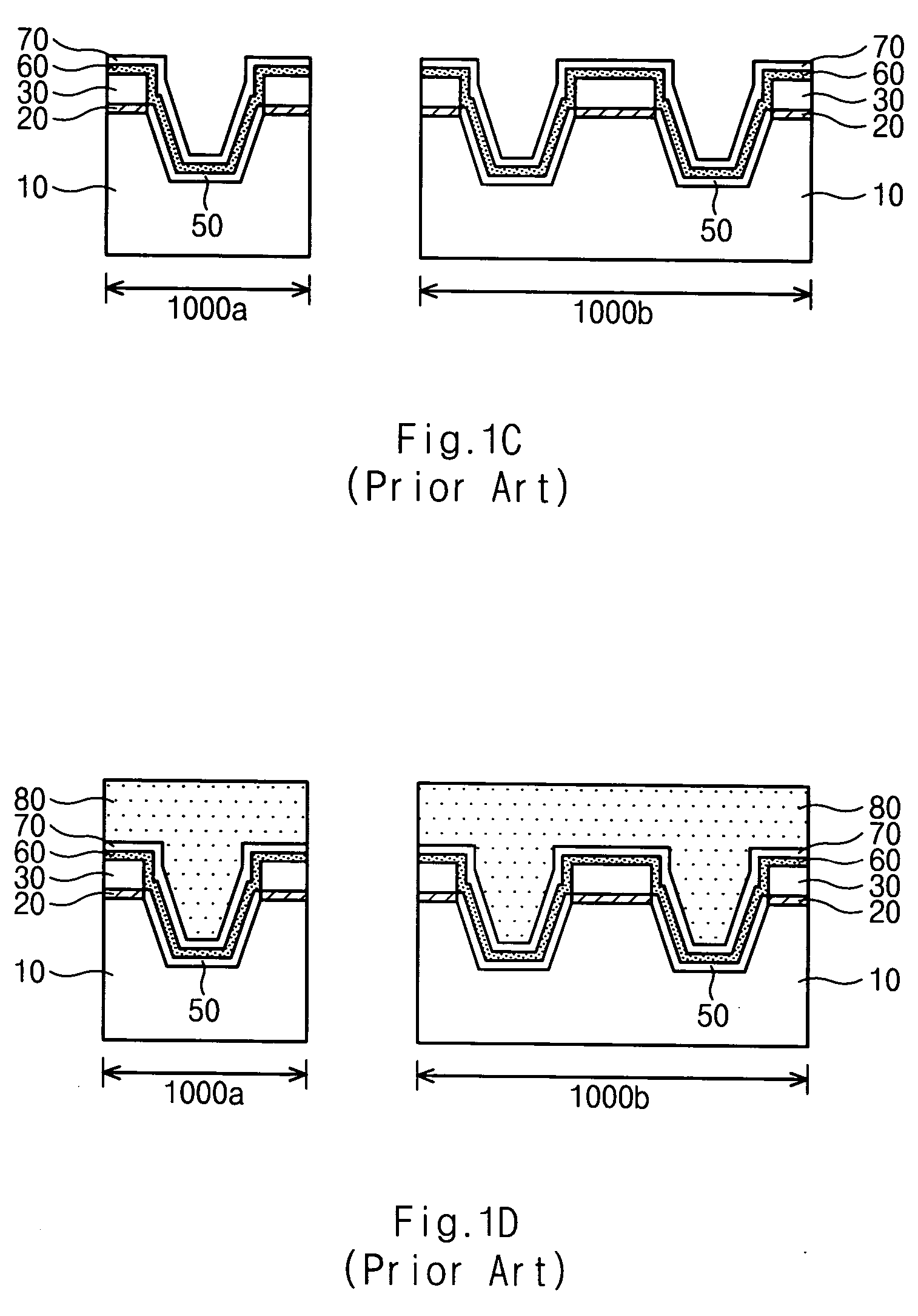
[0024] Referring to FIG. 2c, a sidewall oxide...


PUM


Abstract

A method for manufacturing device isolation film of semiconductor device is disclosed. The method utilizes a plasma oxidation of a liner nitride film exposed by etching a liner oxide the film in peripheral region prior to the formation of device isolation film to prevent the generation of a electron trap which causes trapping of electrons at the interface of the oxide film and the nitride film resulting in a HEIP phenomenon.

Description

CORRESPONDING RELATED APPLICATION [0001] This application claims the benefit of and priority to Korean patent application no. ° KR10-2004-0054280, filed on Jul. 13, 2004, the entire contents of which are incorporated by reference herein in its entirety. BACKGROUND OF THE INVENTION [0002] 1. Field of the Invention [0003] The present invention generally relates to a method for manufacturing a device isolation film of a semiconductor device, and more specifically, to a method for manufacturing a device isolation film of a semiconductor device wherein a liner nitride film exposed by etching a liner oxide in a peripheral region is oxidized using plasma prior to the formation of the device isolation film to prevent or reduce a Hot Electron Induced Punchthrough (HEIP) phenomenon and / or to improve characteristics of a semiconductor device. [0004] 2. Description of the Related Art [0005]FIGS. 1a through 1e are cross-sectional diagrams illustrating a conventional method for manufacturing a de...

Claims


Application Information

Patent Timeline
IPC IPC(8): H01L21/76
CPCH01L21/76229Y10S438/954H01L21/823878H01L21/762
Inventor LEE, SANG DON
Owner SK HYNIX INC
Why Eureka
Try Eureka