
Setting black levels in organic EL display devices

a technology of electroluminescent devices and black levels, which is applied in the direction of electroluminescent light sources, static indicating devices, instruments, etc., can solve the problems of accelerating the deterioration of oled elements, unable to compensate for the change of black and/or white levels, and/or display luminance may be reduced, and/or image luminance may increase.

Active Publication Date: 2005-03-10
GLOBAL OLED TECH
View PDF3 Cites 53 Cited by
  • Summary
  • Abstract
  • Description
  • Claims
  • Application Information

AI Technical Summary

Problems solved by technology

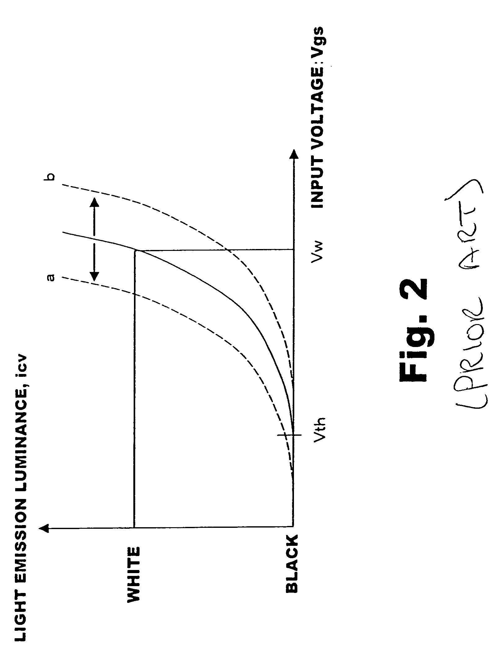
The voltage Vth, however, is likely to change due to a change in temperature or external light.
Moreover, an excessive current may flow into the panel, which may accelerate deterioration of an OLED element.
This method, however, cannot compensate for a change in a black and / or white level caused due to an environmental change, as it can only limit a current flowing in the display panel.
Thus, an appropriate display cannot be maintained should an environmental condition be changed.

Method used


Image

  • Setting black levels in organic EL display devices
  • Setting black levels in organic EL display devices
  • Setting black levels in organic EL display devices

Examples


Embodiment Construction

[0026] In the following, preferred embodiments of the present invention will be described with reference to the following drawings.

[0027]FIG. 3 shows a structure of a device of a preferred embodiment of the present invention. In this device, a video signal including image data for each pixel is input to a gamma correction circuit 10 for correcting a video signal according to predetermined gamma propriety so that the resultant image data has linear relationship with an amount of a current flowing in a pixel. A video signal subjected to gamma correction is supplied to an adder 12 for addition of a black level setting level, so that an output of the adder 12 resultantly constitutes data concerning a driving current for each pixel.

[0028] The output of the adder 12 is supplied to a D / A converter 14 for conversion into an analog signal, which is supplied to an organic EL panel 16, which includes pixel circuits, as shown in FIG. 1, arranged in a matrix.

[0029] Note that a signal from the...


PUM


Abstract

To appropriately adjust luminance and a black level even when characteristics of an organic EL display element should be changed due to an environmental change or heat self-generation, to display a stable image. A current detector detects a level of a total panel current flowing in an organic EL panel. The detected level is subjected to A / D conversion before being supplied to an adder. Meanwhile, a video signal is supplied to a current calculator 24 to be converted into data corresponding to the level of a total panel current, before being supplied to the adder. The adder then compares an average total panel current level, estimated based on a video signal, and an actual total panel current level, to obtain a difference so that a black level for image data to be supplied to the panel is adjusted according to the difference.

Description

FIELD OF THE INVENTION [0001] The present invention relates to setting of a black level in an organic electroluminescent (EL) device. BACKGROUND OF THE INVENTION [0002]FIG. 1 shows an example of a circuit structure for one pixel of an active-type organic EL display device (a pixel circuit). In this structure, a driving thin film transistor (TFT 1) of a P-channel type is connected, via its drain, to an anode of an organic EL element 3, via its source, to a power source line PVdd, and, via its gate, to a source of a selecting thin film transisitor (TFT 2) of an N-channel type. The organic EL element 3 is further connected, via its cathode, to a cathode power source CV. The selected TFT 2 is further connected, via its drain, to a data line Data and, via its gate, to a gate line Gate. The gate of the driving TFT 1 is also connected to one end of a holding capacitor C, which is further connected, on its other end, to a capacitor power source line Vsc. [0003] The gate line, which runs in ...

Claims


Application Information

Patent Timeline
Patent Type & Authority Applications(United States)
IPC IPC(8): G09G3/20H01L51/50G09G3/30G09G3/32H05B33/14
CPCG09G3/3233G09G3/3291G09G2300/0809G09G2300/0842G09G2310/027G09G2360/16G09G2320/029G09G2320/04G09G2320/041G09G2320/0626G09G2360/144G09G2320/0238
Inventor MIZUKOSHI, SEIICHIMORI, NOBUYUKIONOMURA, KOUICHIKOHNO, MAKOTO
Owner GLOBAL OLED TECH
Learn More