Multi-package conversion kit for a pick and place handler

a multi-package, pick-and-place technology, applied in the direction of manufacturing tools, other domestic articles, other manufacturing equipment/tools, etc., can solve the problems of increasing the overall manufacturing cycle time, requiring different vacuums for different sizes of a common package, and requiring different input arms for each package/siz

Inactive Publication Date: 2004-07-15
STATS CHIPPAC LTD
View PDF9 Cites 3 Cited by
  • Summary
  • Abstract
  • Description
  • Claims
  • Application Information

AI Technical Summary

Benefits of technology

[0007] It is another object of the present invention to provide an economical method and device for converting a pick and place handler to accommodate various semiconductor packages and / or sizes.
[0008] It is yet another object of the present invention to provide a method for converting a pick and place handler to accommodate various semiconductor packages and / or sizes with reduced conversion and set-up time.
[0009] To accomplish the above objectives, the present invention provides a method and conversion kit which can be used to convert a pick and place handler for a different semiconductor package economically, and with minimum conversion and set-up time. An input arm assembly is provided with interchangeable vacuum leads such that package-to-package conversion only requires replacing the vacuum lead with a different size vacuum lead. An input / output shuttle plate is provided comprising a block and base plate. The block has a plurality of pocket groupings and a two or more alignment hole groupings. The base plate has two or more alignment pins. Package-to-package conversion is achieved by changing which alignment hole in each alignment hole grouping is set on the alignment pins, thereby selecting the pocket in each pocket grouping corresponding to the alignment hole used. A soak plate is provided having an array of pocket groupings, wherein each pocket grouping has the same pattern of different size / shape pockets to accommodate different packages. Package-to-package conversion is accomplished by programming an offset to the desired pocket in each pocket grouping. An test arm assembly is provided with interchangeable vacuum leads and interchangeable nest pieces such that package-to-package conversion only requires replacing the vacuum lead and nest piece with a different size vacuum lead and nest piece.
[0010] The present invention provides considerable improvement over the prior art. Setup time is reduced because the input arm assembly and test arm assembly can be converted by changing the interchangeable vacuum lead and the interchangeable nest piece as required, instead of changing the entire input arm assembly and the entire test arm. Set-up time is also reduced by the soak plate and input / output shuttle plate which can accommodate different packages, eliminating the need to replace them. Tool inventory and maintenance cost is reduced because separate input arm assemblies, test arm assemblies, soak plates, and input / output shuttle plates do not need to be provided and maintained for each package that the pick and place handler is to be used with.

Problems solved by technology

However, different packages and even different sizes of a common package can require different vacuum leads.
Maintaining a different input arm for each package / size is expensive, and the conversion time can increase overall manufacturing cycle time.
Another problem with converting a pick and place handler to a different package / size semiconductor device is that holding fixtures (e.g. soak buffers and I / O shuttle plates, shown in FIGS. 2 and 3 respectively) must be changed to accommodate the new package / size.
Again, maintaining different fixtures for each package / size is expensive.
Also, the conversion process adversely effects manufacturing cycle time.
Yet another problem with converting a pick and place handler to a different package / size semiconductor device is that a new test arm assembly, as shown in FIG. 4, is required.
Maintaining test arms for each package / size is expensive.
The conversion process adversely effects manufacturing cycle time.
The problem with the prior art conversion kits for pick and place handlers is that they require an expensive collection of assembly arm, fixtures and test arms.
Also, set-up times for converting the replacement input arm, fixtures, and test arm adversely effect manufacturing cycle time.

Method used


Image

  • Multi-package conversion kit for a pick and place handler
  • Multi-package conversion kit for a pick and place handler
  • Multi-package conversion kit for a pick and place handler

Examples


Embodiment Construction

--FIGS. 5-9

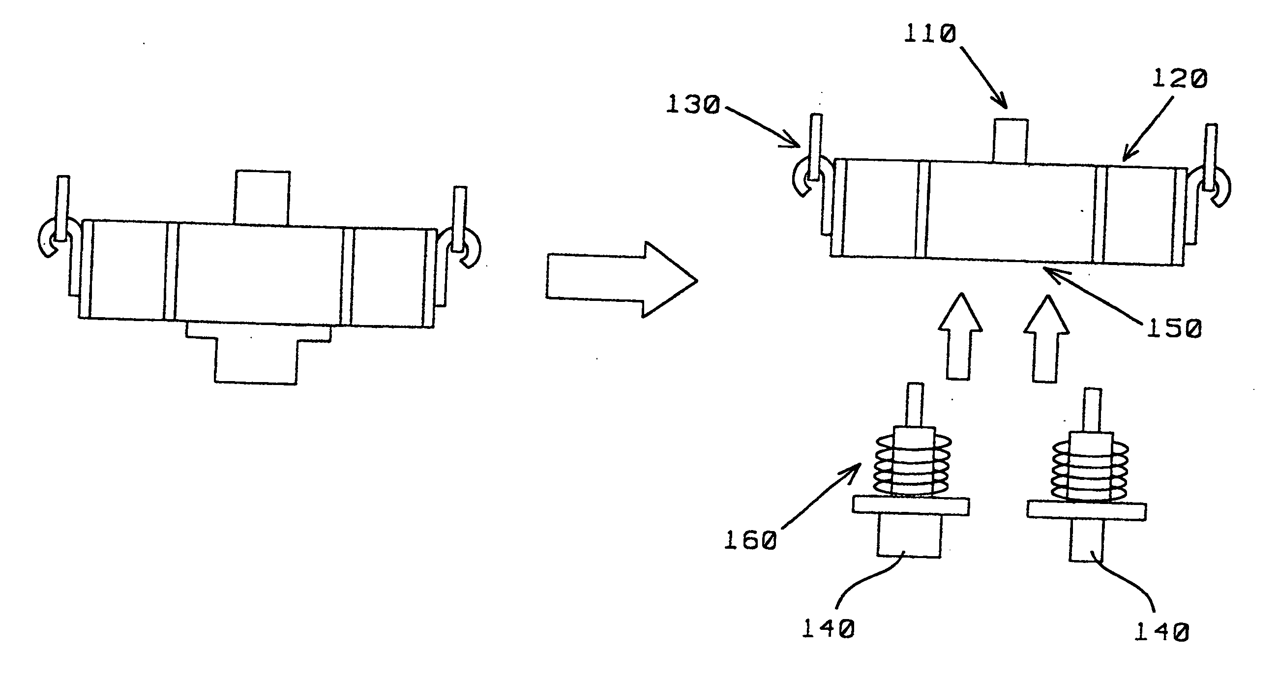
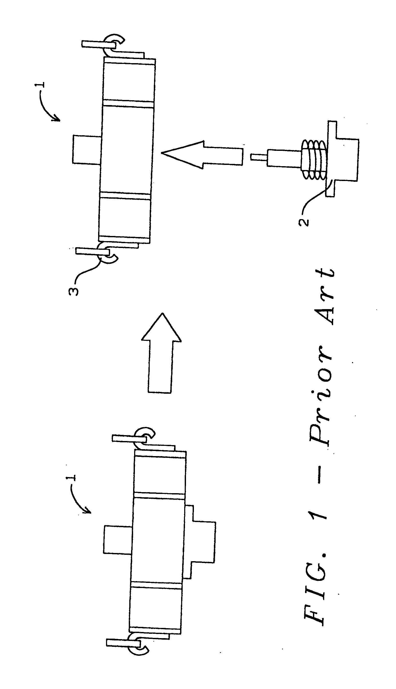
[0029] Referring to FIG. 5, the preferred embodiment of the present invention begins by providing an input arm assembly (100). The input arm assembly comprises a pressure fitting (110), an input arm body (120), input arm clips (130), and a vacuum lead (140) selected from a set of interchangeable vacuum leads having different sizes. The correct size vacuum lead (140) for the semiconductor device to be picked and placed, is inserted in a through hole (150) in the input arm body (120). The vacuum lead (140) is retained by a set screw on the pressure fitting (110).

[0030] Each vacuum lead (140) has an upper hollow cylindrical portion and a lower hollow cylindrical portion with a flange therebetween. The upper cylindrical portion is inserted into the through hole (150) in the input arm body (120). The lower cylindrical portion is moved proximate to a semiconductor device, such that vacuum pressure drawn through the vacuum lead lifts and holds the semiconductor device. A compres...


PUM


Abstract

The present invention provides a kit and method for package-to-package conversion of a pick and place handler. An input arm assembly is provided with interchangeable vacuum leads such that package-to-package conversion only requires replacing the vacuum lead with a different size vacuum lead. An input / output shuttle plate is provided comprising a block and base plate. The block has a plurality of pocket groupings and a two or more alignment hole groupings. The base plate has two or more alignment pins. Package-to-package conversion is achieved by changing which alignment hole in each alignment hole grouping is set on the alignment pins, thereby selecting the pocket in each pocket grouping corresponding to the alignment hole used. A soak plate is provided having an array of pocket groupings, wherein each pocket grouping has the same pattern of different size / shape pockets to accommodate different packages. Package-to-package conversion is accomplished by programming an offset to the desired pocket in each pocket grouping. An test arm assembly is provided with interchangeable vacuum leads and interchangeable nest pieces such that package-to-package conversion only requires replacing the vacuum lead and nest piece with a different size vacuum lead and nest piece.

Description

BACKGROUND OF INVENTION[0001] 1) Field of the Invention[0002] This invention relates generally to surface mount assembly of semiconductor devices and more particularly to a method and device for converting a pick and place handler for use with devices having different packages and / or different sizes.[0003] 2) Description of the Prior Art[0004] Pick and place handlers are widely used in surface mount technology for physically moving semiconductor devices during assembly and test. A vacuum lead is typically used to pick up a semiconductor device and hold it during transport to a new location (e.g. a circuit board or a holding fixture). However, different packages and even different sizes of a common package can require different vacuum leads.[0005] The importance of overcoming the various deficiencies noted above is evidenced by the extensive technological development directed to the subject, as documented by the relevant patent and technical literature. The closest and apparently mor...

Claims


Application Information

Patent Timeline
Patent Type & Authority Applications(United States)
IPC IPC(8): H05K13/04
CPCH05K13/0408H05K13/0465Y10T29/49716Y10T29/53191Y10T29/5313H05K13/0409
Inventor SUM, KAI WAHTAN, WEE BOONYAP, LIOP JIN
Owner STATS CHIPPAC LTD
Why Eureka
Try Eureka