
Display panel

a display panel and display panel technology, applied in the field of display panels, can solve the problems of high production cost of display panels, difficult manufacturing of fine metal masks (fmm), large differences in display and uneven display, etc., and achieve good display quality performance, reduce the aperture ratio of metals of transparent display areas, and reduce the effect of display quality performan

Active Publication Date: 2022-04-05
WUHAN CHINA STAR OPTOELECTRONICS SEMICON DISPLAY TECH CO LTD
View PDF18 Cites 2 Cited by
  • Summary
  • Abstract
  • Description
  • Claims
  • Application Information

AI Technical Summary

Benefits of technology

The present patent solves the problem of reducing display quality performance in a transparent display area by using a density of sub-pixel units that is the same as a conventional display area, resulting in better display uniformity and reduced production costs. Additionally, the reduced aperture ratio of metal in the transparent display area improves light transmittance, while the size of the TFT circuit and the use of transparent electrode materials further enhance the light capturing capability and imaging quality performance of the camera component. Finally, the increased screen-to-body ratio in the display device is beneficial for a full screen design.

Problems solved by technology

The above technical solution can achieve the purpose of improving the light transmittance and improving imaging quality performance of a camera, but it will affect display quality performance of the transparent display area, causing a large difference on display and uneven display.
Moreover, due to the different pixel densities of the transparent display area and a conventional display area, a fine metal mask (FMM) is difficult to manufacture, and the display panel has a higher production cost.

Method used


Image

  • Display panel
  • Display panel
  • Display panel

Examples


Embodiment Construction

[0036]The technical solutions according to the embodiments of the present disclosure are described clearly and completely in conjunction with accompanying drawings in the embodiments of the present disclosure. Apparently, the described embodiments are only a part rather than all the embodiments of the present disclosure. All other embodiments obtained by those skilled in the art without creative efforts based on the embodiments of the present disclosure fall within the protection scope of the present disclosure.

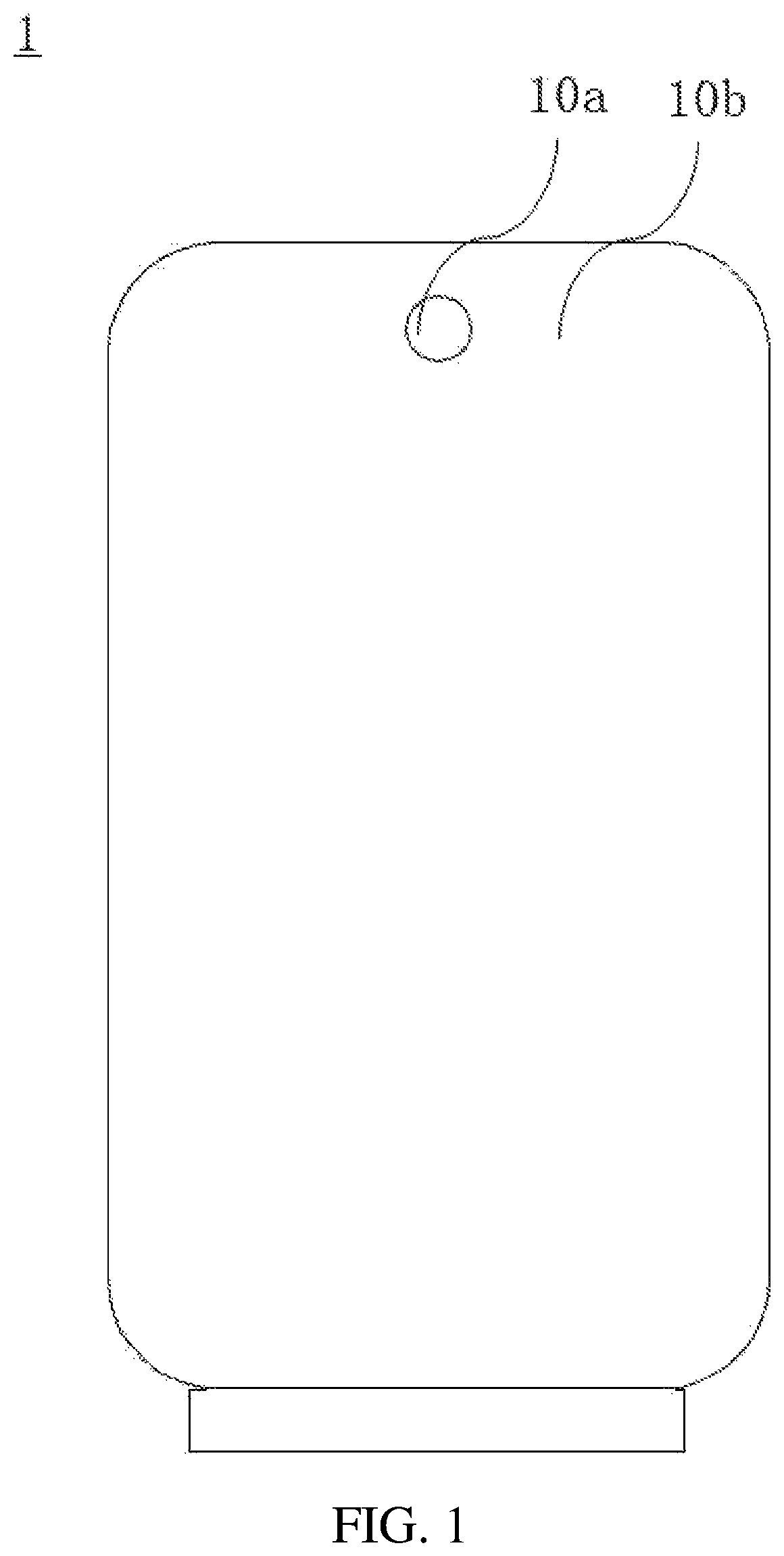
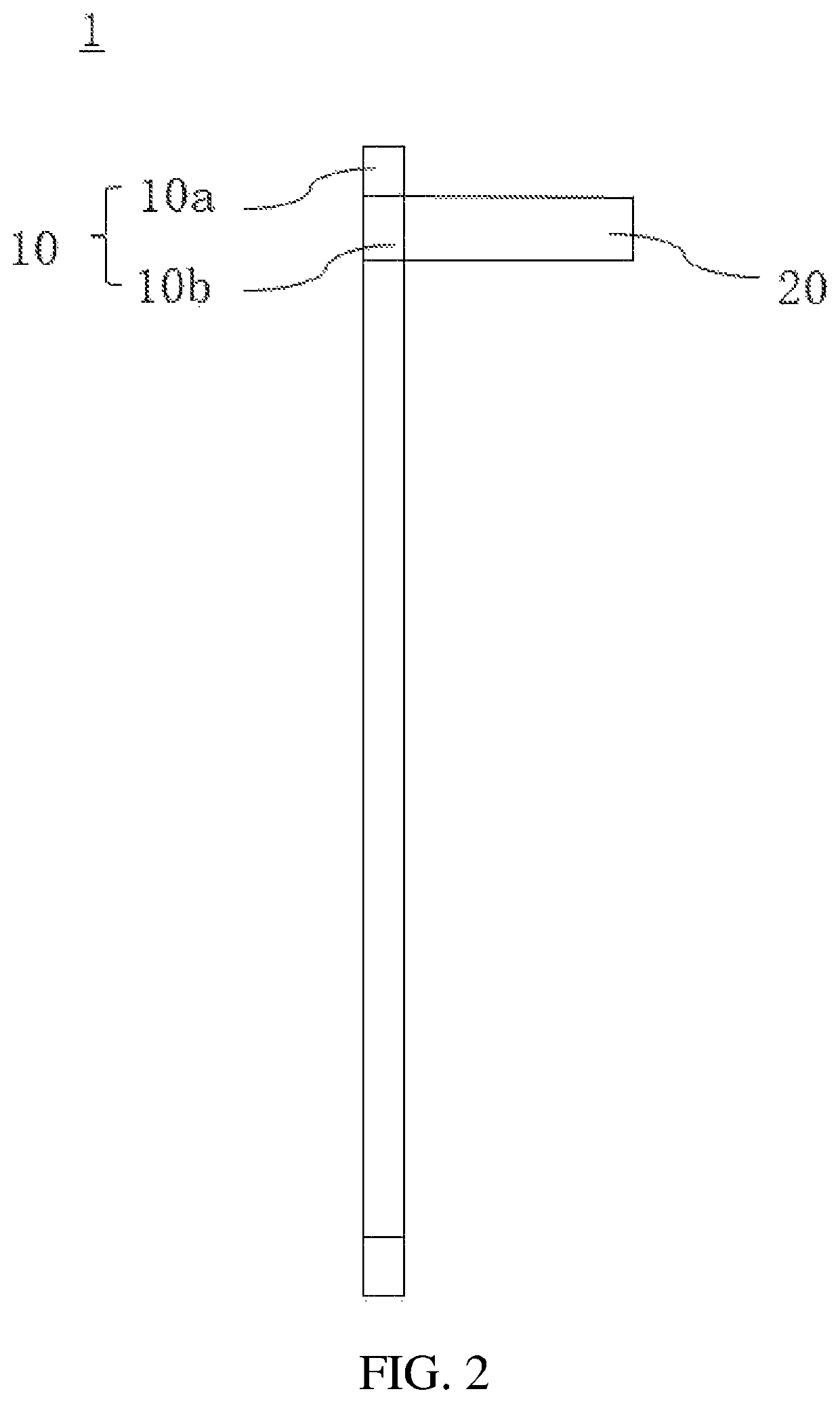
[0037]As shown in FIG. 1 and FIG. 2, the present disclosure provides a display panel 10 having a transparent display area 10a and a conventional display area 10b surrounding the transparent display area 10a.

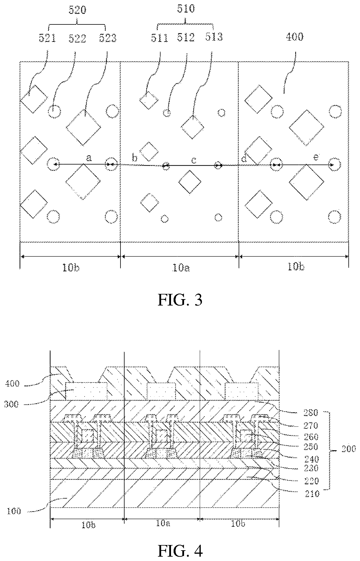
[0038]Referring to FIG. 3, the transparent display area 10a includes a plurality of first sub-pixel units 510, and the conventional display area 10b includes a plurality of second sub-pixel units 520. A density of first sub-pixel units 510 in the transparent display area ...


PUM


Abstract

A display panel is provided, including a transparent display area and a conventional display area surrounding the transparent display area. The transparent display area and the conventional display area both include a plurality of sub-pixel units, and a density of sub-pixel units in the transparent display area is the same as a density of sub-pixel units in the conventional display area. A pixel area of the sub-pixel units in the transparent display area is less than a pixel area of the sub-pixel units in the conventional display area.

Description

FIELD OF DISCLOSURE[0001]The present disclosure relates to the field of display technologies, and in particular, to a display panel and a display device with a high light transmittance of a transparent display area.BACKGROUND[0002]Organic light-emitting diodes (OLEDs) have advantages of self-illumination, high contrast, wide viewing angles, low power consumption, and flexibility, so they are popular among people and developers. Flexible OLED is gradually occupying a market due to its remarkable resistance against bending force and thinness. On this basis, a display device with a high screen-to-body ratio and a full-screen has also become focus of development and research and development trends of market.[0003]Taking a display panel of a mobile phone as an example, increasing a screen-to-body ratio of the display panel of the mobile phone and an aesthetic appearance of the mobile phone have become a mainstream design of a screen of the mobile phone. However, in addition to a display ...

Claims


Application Information

Patent Timeline
Patent Type & Authority Patents(United States)
IPC IPC(8): H01L27/32H01L51/52
CPCH01L27/3218H01L27/3234H01L27/3262H01L51/5234H01L2251/308H10K59/352H10K59/65H10K59/1213H10K59/80524H10K59/353H10K59/121H10K59/122H10K50/828H10K2102/103
Inventor ZHANG, MINGYANG, JIE
Owner WUHAN CHINA STAR OPTOELECTRONICS SEMICON DISPLAY TECH CO LTD
Learn More