
Multi-port memory device with serial input/output interface

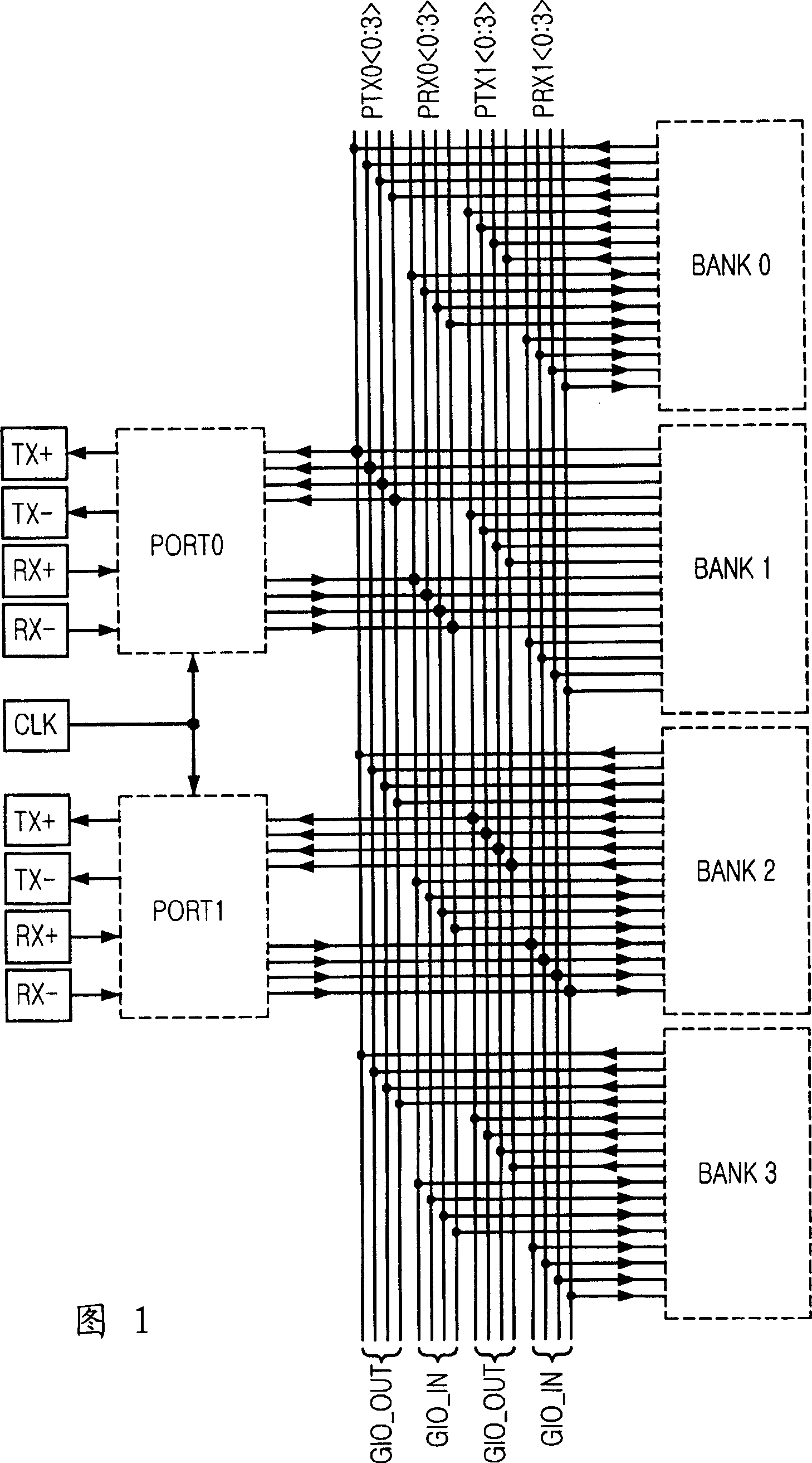
A memory and multi-port technology, applied in static memory, digital memory information, information storage, etc., can solve the problems of weakening product competitiveness, increasing manufacturing cost, and large investment

Inactive Publication Date: 2007-04-04
SK HYNIX INC
View PDF0 Cites 7 Cited by
  • Summary
  • Abstract
  • Description
  • Claims
  • Application Information

AI Technical Summary

Problems solved by technology

[0029] In this situation, traditional test equipment used to test typical DRAM devices has limitations in transmitting and recognizing high-speed data signals
Therefore, it is difficult to verify the operation of multi-port memory devices, so that high-speed test equipment is required
However, since the introduction of high-speed test equipment requires a large investment, the unit manufacturing cost increases and the competitiveness of products decreases accordingly

Method used


Image

  • Multi-port memory device with serial input/output interface
  • Multi-port memory device with serial input/output interface
  • Multi-port memory device with serial input/output interface

Examples


Embodiment Construction

[0077] Hereinafter, a test interface of a multi-port memory device with a serial input / output (I / O) interface according to an exemplary embodiment of the present invention will be described in detail with reference to the accompanying drawings.

[0078] FIG. 3 is a block diagram of a multi-port memory device according to a first embodiment of the present invention. For ease of illustration, a multi-port memory device with two ports and four memory banks is illustrated.

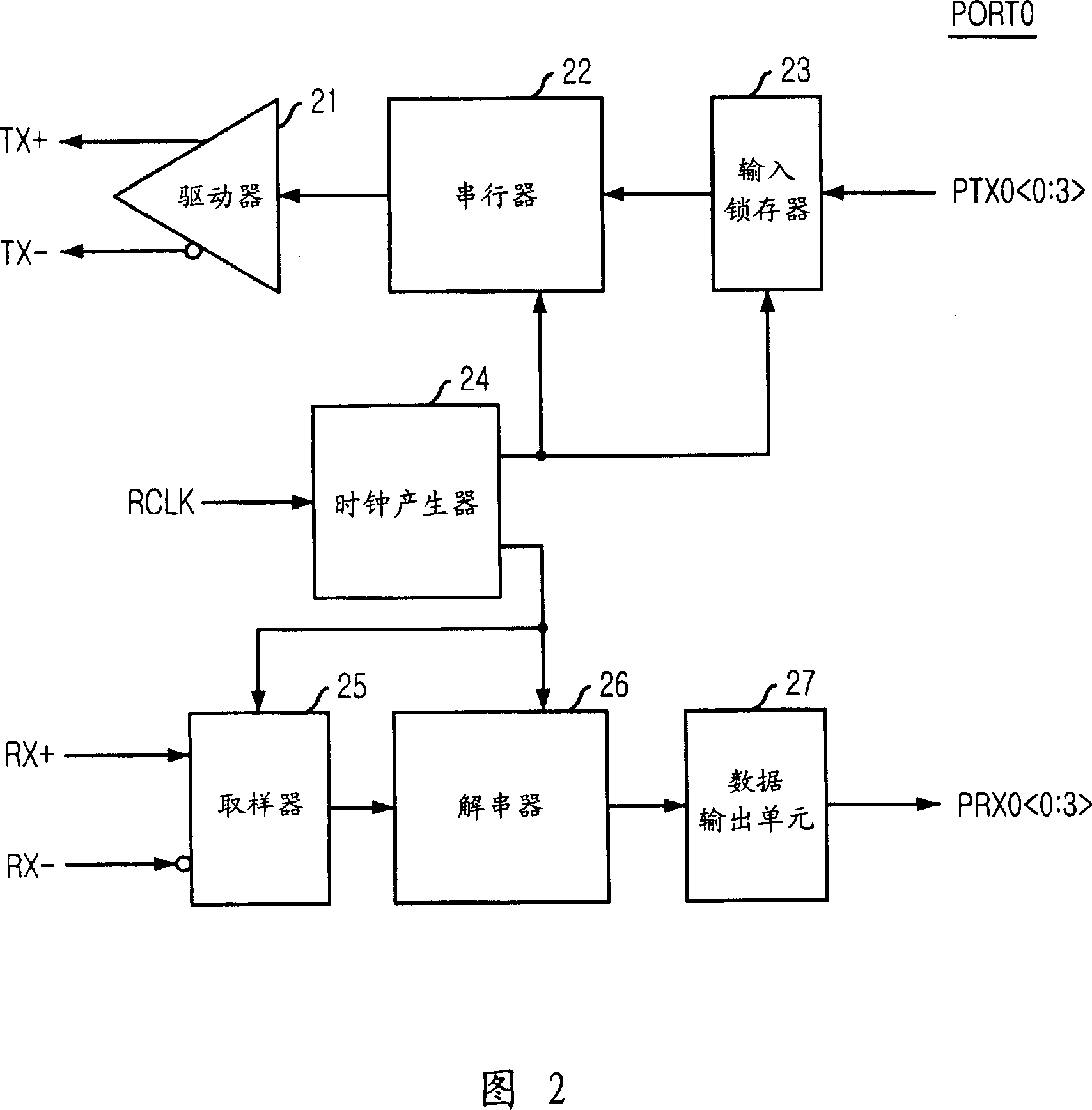
[0079] The multi-port memory device includes: a plurality of serial I / O pads TX0+, TX0-, TX1+, TX1-, RX0+, RX0-, RX1+, and RX1-; a plurality of parallel I / O pads IN, T and OUT; test port TPORT; first selection unit 31 and second selection unit 32; first port PORT0 and second port PORT1; first storage group BANK0 to fourth storage group BANK3 ; and a first global input / output (I / O) data bus GIO_IN and a second global input / output (I / O) data bus GIO_OUT.

[0080] In the high-speed serial I / O interface, a plur...


PUM


Abstract

A multi-port memory device including: a plurality of serial input / output (I / O) data pads; a plurality of parallel I / O data pads; and a plurality of first ports for via the serial I / O a data pad for performing serial I / O data communications with an external device; a plurality of memory banks for performing parallel I / O data communications with the first ports via a plurality of first data buses; and a second port for performing parallel I / O data communications with the external devices via the parallel I / O data pads and performing serial I / O with the first ports via a plurality of second data buses during test mode data communication.

Description

technical field [0001] The present invention relates to a multi-port memory device, and more particularly, to a test interface for a multi-port memory device with a serial input / output (I / O) interface for handling multiple simultaneous operations with an external device . Background technique [0002] In general, most memory devices, including random access memory (RAM), have a single port with multiple sets of input / output pins. That is, a single port is provided for data exchange between the memory device and an external chipset. Such memory devices with a single port use a parallel input / output (I / O) interface to simultaneously transfer multi-bit data via signal lines connected to multiple I / O pins. The memory device exchanges data with external devices via a plurality of I / O pins in parallel. [0003] The I / O interface is an electrical and mechanical system (scheme) that connects unit devices with different functions through signal lines and accurately transmits trans...

Claims


Application Information

Patent Timeline
Patent Type & Authority Applications(China)
IPC IPC(8): G11C7/10G11C29/56
CPCG11C8/16G11C29/1201G11C29/14G11C29/26G11C2207/105
Inventor 都昌镐
Owner SK HYNIX INC
Learn More