
Asymmetric memory cell

A storage unit, asymmetric technology, applied in the direction of information storage, static memory, digital storage information, etc., can solve the problems of impracticality, storage unit not working normally, process tolerance sensitivity and other problems

Inactive Publication Date: 2005-02-02
SHARP KK
View PDF0 Cites 0 Cited by
  • Summary
  • Abstract
  • Description
  • Claims
  • Application Information

AI Technical Summary

Problems solved by technology

However, smaller feature sizes make devices more sensitive to process tolerances
Relatively small geometrically asymmetric devices are not practical due to process tolerances
However, analysis (given below) shows that the fabricated memory cell with sufficient geometric symmetry will not function properly
Even though these geometrically symmetric devices can be programmed, the net resistance change from the high-resistance state to the low-resistance state is relatively low

Method used


Image

  • Asymmetric memory cell
  • Asymmetric memory cell
  • Asymmetric memory cell

Examples


Embodiment Construction

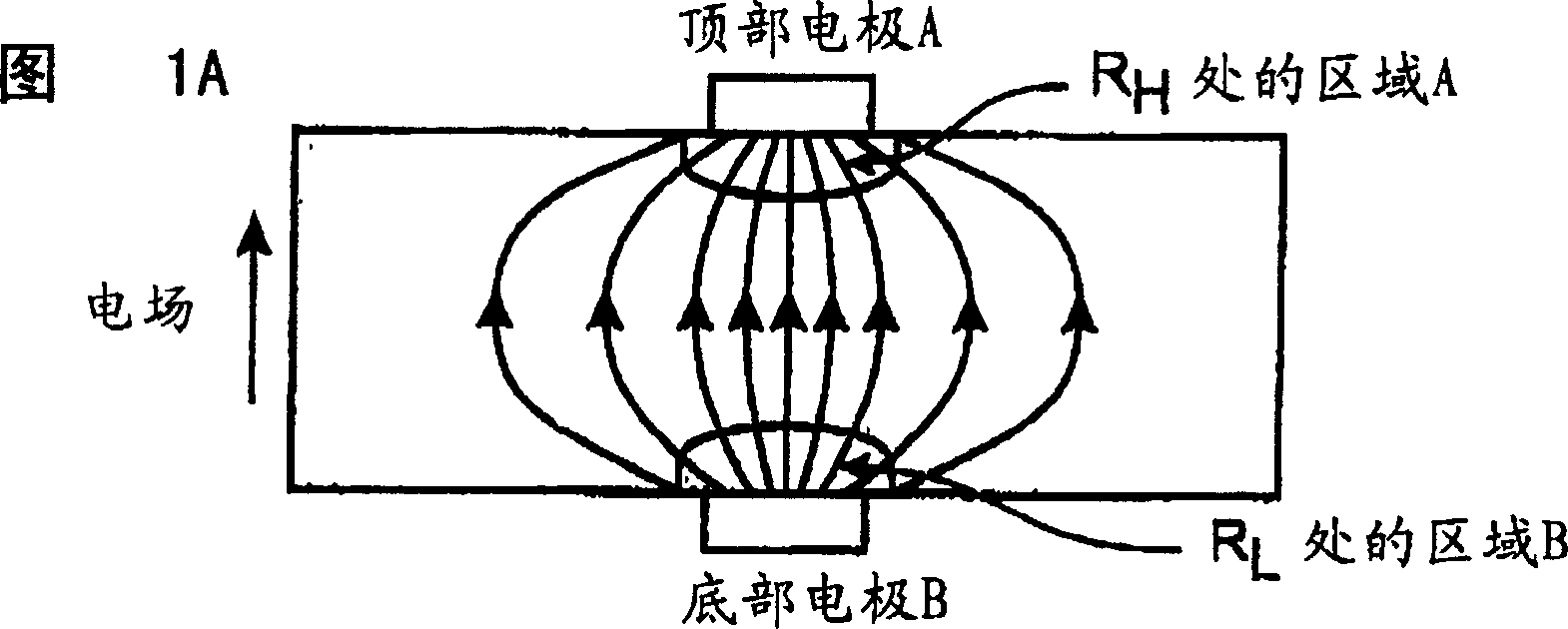
[0016] 1A and 1B are partial cross-sectional views of memory cells during program (FIG. 1A) and erase (FIG. 1B) operations. The top and bottom electrodes are identical, and the storage resistor material is uniform throughout. If the device geometry can be made quite symmetrical, the net resistance will remain constant in the high resistance state when a negative electric field (Fig. 1A) or a positive electric field (Fig. 1B) is applied. Note that the electric field direction is determined with respect to the top electrode. That is, an electric field is believed to be induced from the top electrode. In this case, no programming is possible. Therefore, geometrically symmetric device structures, such as those shown in Figures 1A and 1B, are not practical.

[0017] More specifically, in the presence of an electric field, the geometrically symmetric memory cell has a high current density near the electrodes (regions A and B) and a low current density in the central part of the d...


PUM


Abstract

An asymmetric memory cell and method for forming an asymmetric memory cell are provided. The method comprises: forming a bottom electrode having a first area; forming an electrical pulse various resistance (EPVR) material overlying the bottom electrode; forming a top electrode overlying the EPVR layer having a second area, less than the first area. In some aspects the second area is at least 20% smaller than the first area. The EPVR is a material such as colossal magnetoresistance (CMR), high temperature super conducting (HTSC), or perovskite metal oxide materials. The method further comprises: inducing an electric field between the electrodes; inducing current flow through the EPVR adjacent the top electrode; and, in response to inducing current flow through the EPVR adjacent the top electrode, modifying the resistance of the EPVR. Typically, the resistance is modified within the range of 100 ohms to 10 mega-ohms.

Description

technical field [0001] The present invention relates generally to integrated circuit (IC) memory cell arrays, and more particularly to an asymmetric storage resistive memory cell and method of manufacturing the same. Background technique [0002] Typically, a memory cell using a memory resistor material, such as a very large magnetoresistance (CMR) material, is made with an unpatterned conductive bottom electrode, an unpatterned CMR material, and a relatively small top electrode. These devices work in a limited number of applications, but because of the relatively large size of these memory cells they are not suitable for high density memory array applications. [0003] CMR materials can be said to have non-volatile properties because the resistance of the CMR material remains constant in most cases. However, when a high electric field induces current to flow through the CMR material, it can cause a change in the CMR resistance. During the procedure, the resistivity of the...

Claims


Application Information

Patent Timeline
Patent Type & Authority Applications(China)
IPC IPC(8): H01L27/10G11C11/15G11C13/00H01L21/8246H01L27/105H01L43/08
CPCB82Y10/00G11C2213/31H01L45/1253G11C13/0007H01L45/145G11C11/15G11C2213/52H10N70/20H10N70/841H10N70/8836H10N70/826A47G21/103A47G2400/02
Inventor 许胜籐李廷凯D·R·埃文斯
Owner SHARP KK
Learn More