Athermalized super lens and design method thereof
A design method and metalens technology, applied in the field of optics, can solve problems such as the failure to improve the imaging performance of the metalens, and achieve the effect of improving temperature drift
- Summary
- Abstract
- Description
- Claims
- Application Information
AI Technical Summary
Problems solved by technology
Method used
Image
Examples
Embodiment 1
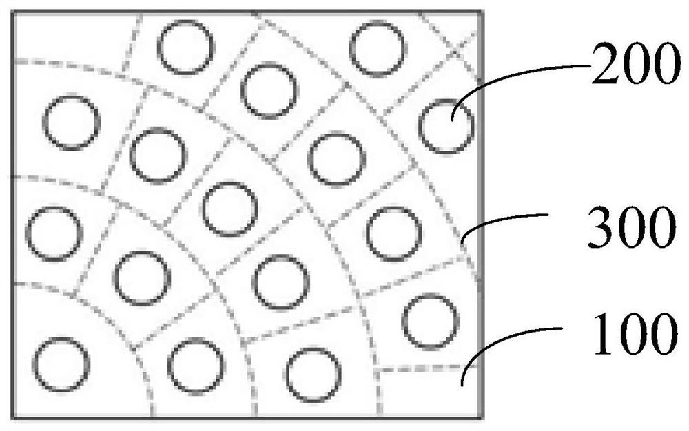
[0097]Exemplarily, an embodiment of the present application provides an athermalized metalens, which includes a quartz substrate and an amorphous silicon nanostructure disposed thereon. The athermalized metalens has an aperture of 1mm, a focal length of 2.5mm, and a working wavelength of 940mm in the near infrared. The material of the nanostructure is amorphous silicon, the height is 500nm, and regular hexagons are arranged as superstructure units. The period of the regular hexagon is 450nm, and the nanostructures are located at the vertices of the regular hexagon. The low temperature threshold of the working environment of the athermalized metalens is -20°C, and the high temperature threshold is 100°C.
[0098] The temperature drift analysis of the athermalized metalens in the 940nm band is as follows.
[0099] Since the operating wavelength is 940nm, the temperature coefficient of refractive index of amorphous silicon is 3x10 -4 / K. Therefore, the refractive indices of t...
Embodiment 2
[0102] Exemplarily, an embodiment of the present application provides another athermalized metalens, including a quartz substrate and a nanostructure disposed thereon. The athermalized metalens has an aperture of 1mm, a focal length of 2.5mm, and a working wavelength of 940mm in the near infrared. The materials of the nanostructure along the direction away from the substrate are sapphire and barium fluoride (see Table 1 for parameters). Calculated according to the formula (1), the height of the barium fluoride in the nanostructure is 715nm, and the height of the sapphire is 785nm. In Example 2, the nanostructures are arranged with regular hexagons as superstructure units. The period of the regular hexagon is 550nm, and the nanostructures are located at the vertices of the regular hexagon. The low temperature threshold of the working environment of the athermalized metalens is -20°C, and the high temperature threshold is 100°C.
[0103] The temperature drift analysis of the ...
PUM
| Property | Measurement | Unit |
|---|---|---|
| height | aaaaa | aaaaa |
| height | aaaaa | aaaaa |
| height | aaaaa | aaaaa |
Abstract
Description
Claims
Application Information
 - R&D
- Intellectual Property
- Life Sciences
- Materials
- Tech Scout
- Unparalleled Data Quality
- Higher Quality Content
- 60% Fewer Hallucinations
Browse by: Latest US Patents, China's latest patents, Technical Efficacy Thesaurus, Application Domain, Technology Topic, Popular Technical Reports.
© 2025 PatSnap. All rights reserved.Legal|Privacy policy|Modern Slavery Act Transparency Statement|Sitemap|About US| Contact US: help@patsnap.com


