Sensor packaging structure
A packaging structure and sensor technology, applied in the direction of electric solid-state devices, semiconductor devices, radiation control devices, etc., can solve the problems of excessively long wire arc, easy wire breakage, wire breakage, etc., and achieve the goal of reducing the probability of wire breakage Effect
- Summary
- Abstract
- Description
- Claims
- Application Information
AI Technical Summary
Problems solved by technology
Method used
Image

Examples
Embodiment 1
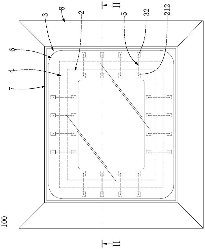
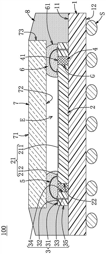
[0028] see figure 1 and figure 2 As shown, it is Embodiment 1 of the present invention. The present embodiment discloses a sensor packaging structure 100, which includes a substrate 1, a sensing chip 2 and a pad layer 3 mounted on the substrate 1 at intervals, located between the sensing chip 2 and the A filling body 4 between the pad layers 3, a plurality of wires 5 connecting the sensing chip 2 and the pad layer 3, a support body 6 arranged on the sensing chip 2 and the pad layer 3 , a light-transmitting layer 7 disposed on the support body 6 , and a packaging body 8 formed on the substrate 1 and surrounding the above-mentioned components.
[0029] Wherein, although the sensor package structure 100 is described as including the above-mentioned components in this embodiment, the sensor package structure 100 can also be adjusted and changed according to design requirements. For example, in other embodiments not shown in the present invention, the sensor packaging structure...
Embodiment 2
[0045] see image 3 and Figure 4 As shown, it is the second embodiment of the present invention. Since this embodiment is similar to the first embodiment above, the similarities between the two embodiments will not be repeated, and the differences between this embodiment and the first embodiment are roughly described as follows:
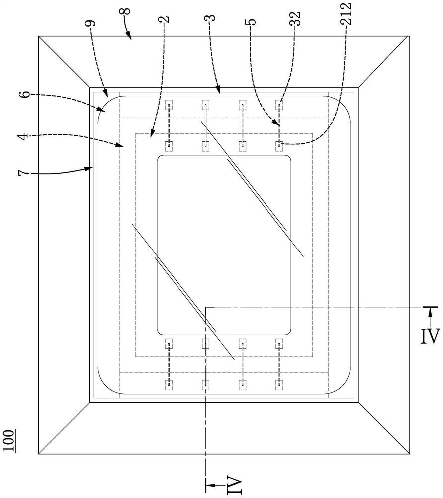
[0046] In this embodiment, the pad layer 3 is not ring-shaped, and the sensor package structure 100 further includes a sealing layer 9 disposed on the first board surface 11, and the sealing layer 9 and the sealing layer 9 The pad layers 3 are connected together to form a ring structure and surround the outer side of the sensing chip 2 . Wherein, the sealing layer 9 is not electrically connected to the substrate 1 and the sensing chip 2, and the top edge of the sealing layer 9 is coplanar with the top edge 31 of the pad layer 3 and the sensing chip. The top surface 21 of the measuring chip 2.
[0047] Further, the sealing layer 9 may be arranged...
Embodiment 3
[0050] see Figure 5 to Figure 7 As shown, it is the third embodiment of the present invention. Since this embodiment is similar to the above-mentioned second embodiment, the similarities between the two embodiments will not be repeated, and the differences between this embodiment and the second embodiment are roughly described as follows:
[0051] In this embodiment, the sealing layer 9 can also be connected to the outer edge 22 of the sensing chip 2, so the filler 4 is only formed between the sensing chip 2 and the pad layer 3 between. The supporting body 6 is ring-shaped and formed on the top edge 31 of the cushion layer 3, the top edge of the sealing layer 9, the top surface 21 of the sensing chip 2, and the filling The top edge 41 of the body 4. Moreover, the support body 6 is not in contact with the sensing region 211 of the sensing chip 2, the outer edge 35 of the pad layer 3, and the outer edge of the sealing layer 9, but the present invention is not limited thereto...
PUM
 Abstract
Description
Claims
Application Information
 - R&D
- Intellectual Property
- Life Sciences
- Materials
- Tech Scout
- Unparalleled Data Quality
- Higher Quality Content
- 60% Fewer Hallucinations
Browse by: Latest US Patents, China's latest patents, Technical Efficacy Thesaurus, Application Domain, Technology Topic, Popular Technical Reports.
© 2025 PatSnap. All rights reserved.Legal|Privacy policy|Modern Slavery Act Transparency Statement|Sitemap|About US| Contact US: help@patsnap.com