Multi-axis cooperative blind milling method for printed circuit board and device

A technology for printed circuit boards and circuit boards, which is applied in milling machine equipment, manufacturing tools, details of milling machine equipment, etc., can solve the problems that the depth of step grooves cannot be unified, the depth of product grooves cannot be realized, and the depth control accuracy is difficult to coordinate, etc. Positioning speed and paste speed, low cost, and the effect of improving efficiency

Active Publication Date: 2021-11-05
湖南省方正达电子科技有限公司
View PDF10 Cites 0 Cited by
  • Summary
  • Abstract
  • Description
  • Claims
  • Application Information

AI Technical Summary

Problems solved by technology

In the mass production of printed circuit boards, 4-axis or 6-axis milling machines are generally used to process step grooves, and the height of the milling cutters on each axis on a multi-axis milling machine is limited by the assembly accuracy of the machine tool itself, or due to the thickness of the processed circuit board itself. Subtle differences will lead to inconsistent step groove depths processed in batches, and the difference in depth control accuracy is often difficult to coordinate. It is impossible to achieve the groove depth (or excess thickness) accuracy of products produced by each axis to meet the requirements of + / -0.1mm
However, if the single-axis operation is adopted, although the groove depth can be guaranteed to be uniform, the production efficiency of the operation is low and the production capacity is wasted.
There is currently no better way to solve this problem

Method used


Image

  • Multi-axis cooperative blind milling method for printed circuit board and device
  • Multi-axis cooperative blind milling method for printed circuit board and device
  • Multi-axis cooperative blind milling method for printed circuit board and device

Examples


Embodiment Construction

[0041] In order to make the above objects, features and advantages of the present invention more comprehensible, specific implementations of the present invention will be described in detail below. In the following description, numerous specific details are set forth in order to provide a thorough understanding of the present invention. However, the present invention can be implemented in many other ways different from those described here, and those skilled in the art can make similar improvements without departing from the connotation of the present invention, so the present invention is not limited by the specific implementation disclosed below.

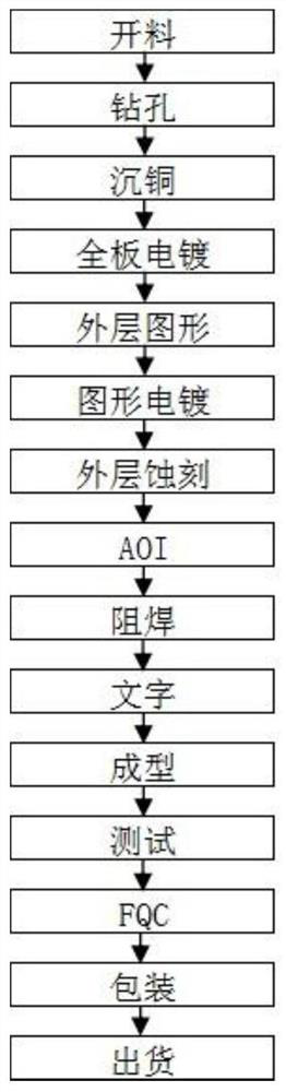
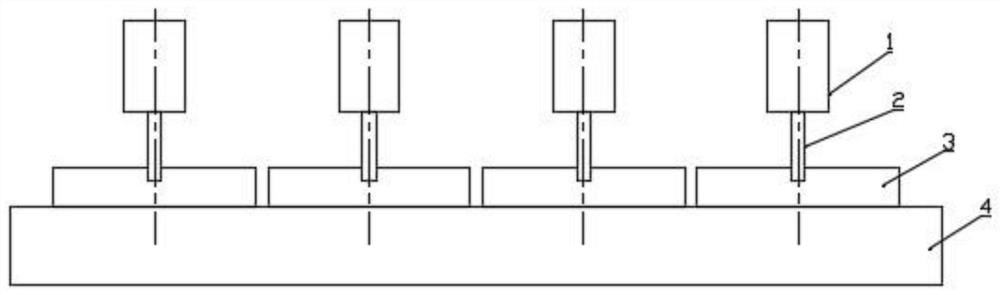
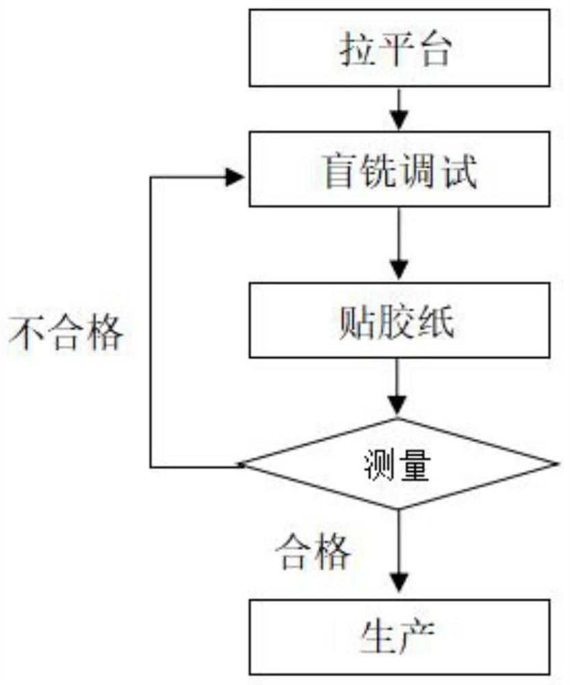
[0042] see Figure 3 to Figure 5 As shown, as an embodiment of a multi-axis collaborative blind milling method for a printed circuit board, the following processing steps are included:

[0043] Pulling the platform: on the worktable 4 of the multi-axis milling machine, lay a backing plate 5 in the area corresponding to each spind...


PUM


Abstract

The invention relates to the technical field of printed circuit board machining, in particular to a multi-axis cooperative blind milling method for a printed circuit board. The multi-axis cooperative blind milling method comprises the following machining steps that a platform is drawn, specifically, base plates are laid on a working table board, and the reference height from main shafts to the upper surfaces of the base plates is kept uniform; blind milling debugging is carried out, specifically, in the blind milling process, the depths of blind grooves are tracked and measured, and when the blind groove meets the depth and precision requirements for the first time, the thickness of the base plate corresponding to the blind groove serves as the reference thickness; adhesive paper sticking is carried out, specifically, the depths of the rest blind grooves of the circuit board which do not meet the machining depth requirement are measured, the depth difference is calculated, and one or more layers of adhesive paper are stuck on the positions of the corresponding base plates according to the depth difference till the depths of the blind grooves machined under all the main shafts are consistent. According to the multi-axis cooperative blind milling method for the printed circuit board, under the condition of full use of multiple shaft joint operation, the precision of the groove depth (or residual thickness) of a product produced by each shaft still meets the requirement of + / -0.1 mm, the production efficiency is improved, the production cost is reduced, and operation is easy, practical and efficient.

Description

technical field [0001] The invention relates to the technical field of printed circuit board processing, in particular to a method and device for multi-axis collaborative blind milling of printed circuit boards. Background technique [0002] Printed circuit boards, also known as printed circuit boards, are providers of electrical connections for electronic components. Printed circuit boards are often represented by "PCB". The design of the printed circuit board is mainly the layout design. The main advantage of using the circuit board is to greatly reduce the errors of wiring and assembly, and improve the automation level and production labor rate. According to the number of layers of circuit boards, it can be divided into single-sided boards, double-sided boards, four-layer boards, six-layer boards and other multi-layer circuit boards. [0003] The existing processing flow chart of printed circuit board is as follows: figure 1 As shown, after material cutting, drilling, ...

Claims


Application Information

Patent Timeline
Patent Type & Authority Applications(China)
IPC IPC(8): B23C3/28B23C9/00
CPCB23C3/28B23C9/00Y02P90/02
Inventor 李长生田德琴方笑求沈兴林
Owner 湖南省方正达电子科技有限公司
Why Eureka
Try Eureka