Semiconductor manufacturing method and multi-piece deposition equipment

A technology of deposition equipment and manufacturing method, applied in semiconductor/solid-state device manufacturing, gaseous chemical plating, coating, etc., can solve the problems of shortening radio frequency generation time, long radio frequency generation time, reducing substrate production efficiency, etc. Radio frequency generation time, the effect of improving production efficiency

Active Publication Date: 2021-10-22
CHANGXIN MEMORY TECH INC
View PDF10 Cites 0 Cited by
  • Summary
  • Abstract
  • Description
  • Claims
  • Application Information

AI Technical Summary

Problems solved by technology

[0003] However, the inventors of the present invention found that, for multi-wafer deposition equipment, even if the deposition process for each batch of substrates is continuously performed, each batch of substrates The interval between the deposition processes of the bottom is much longer than that of the single-chip deposition equipment, resulting in a large reduction in the amount of residual charges in the deposition equipment. Even if the radio frequency compensation function is used to shorten the generation time of radio frequency, the generation time of radio frequency is still very long, seriously Affects the deposition efficiency of multi-wafer deposition equipment, thereby reducing the production efficiency of substrates

Method used


Image

  • Semiconductor manufacturing method and multi-piece deposition equipment
  • Semiconductor manufacturing method and multi-piece deposition equipment
  • Semiconductor manufacturing method and multi-piece deposition equipment

Examples


Embodiment Construction

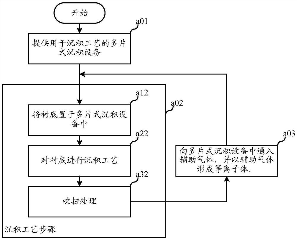
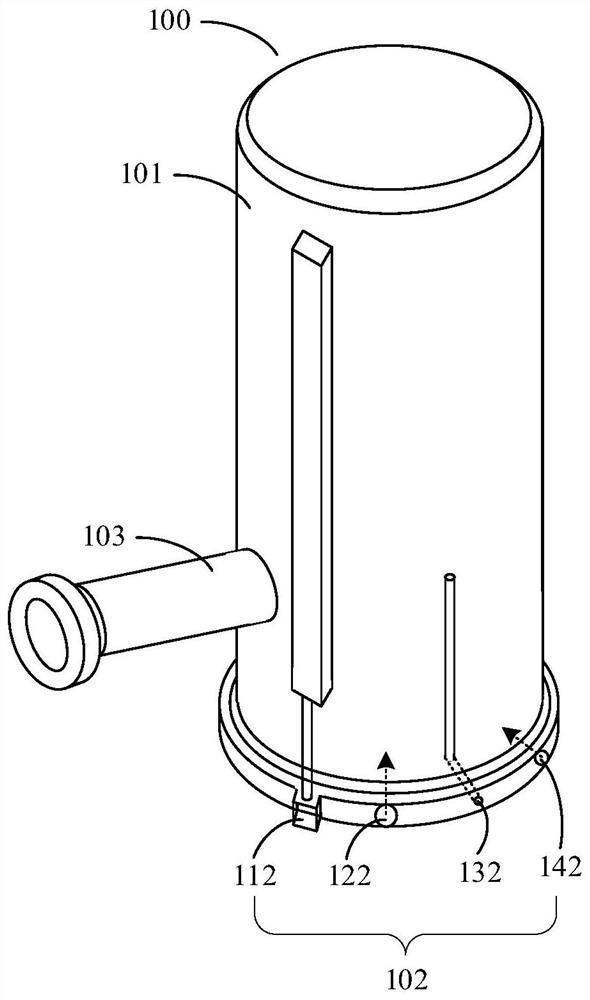
[0030] At present, the equipment used for substrate deposition is divided into single-chip deposition equipment and multi-chip deposition equipment. Compared with single-chip deposition equipment, multi-chip deposition equipment can perform deposition processes on a large number of substrates at a time. The deposition efficiency is higher. In the prior art, the radio frequency compensation function is usually used to shorten the generation time of radio frequency in the multi-chip deposition equipment.

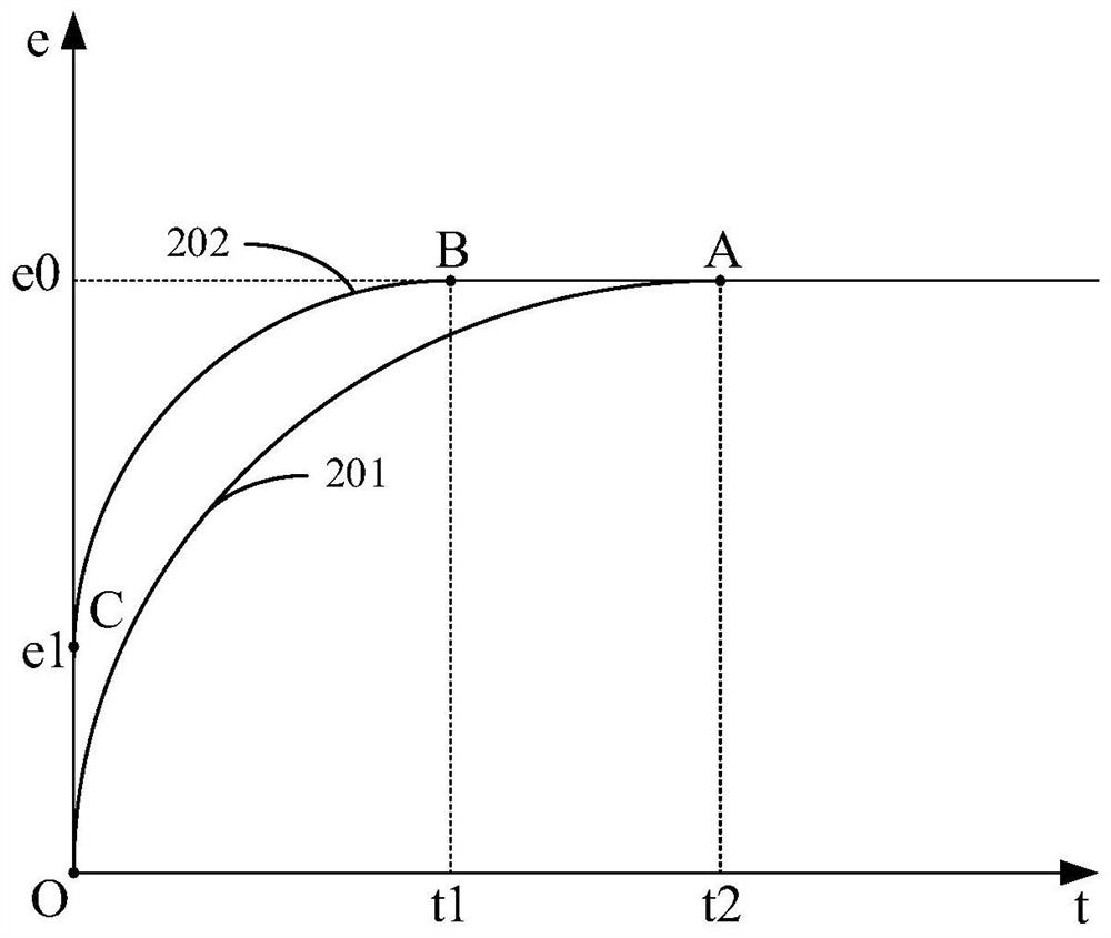
[0031] However, the inventors have found that the reaction space of multi-chip deposition equipment is much larger than that of general single-chip deposition equipment. Therefore, compared with single-chip deposition equipment, multi-chip deposition equipment is a large-volume deposition equipment. And for the multi-chip deposition equipment, even if the deposition process of each batch of substrates is carried out continuously, the interval time between the deposition proce...


PUM


Abstract

The embodiment of the invention provides a semiconductor manufacturing method and multi-piece type deposition equipment. The semiconductor manufacturing method comprises the following steps of performing a first round of deposition process on a substrate in the multi-piece type deposition equipment; taking out the substrate after the first round of deposition process is completed; introducing auxiliary gas into the multi-piece type deposition equipment, and forming plasma by the auxiliary gas; placing a substrate to be deposited into the multi-piece type deposition equipment; and performing a second round of deposition process on the substrate in the multi-piece type deposition equipment. According to the method, in a time interval of the waiting time of the first round of deposition process and the second round of deposition process, the auxiliary gas is introduced to be converted into the plasma, so that the quantity of residual charges in the multi-piece type deposition equipment is increased; and when the second round of deposition process starts, the quantity of the residual charges in the multi-piece type deposition equipment is relatively large, the radio frequency required by the deposition process can be quickly generated, and the generation time of the radio frequency is greatly shortened, so that the production efficiency of the substrate is improved.

Description

technical field [0001] The invention relates to the field of semiconductor manufacturing methods, in particular to a semiconductor manufacturing method and multi-chip deposition equipment. Background technique [0002] At present, the volume of equipment used for substrate deposition is gradually expanding. Large-volume deposition equipment, that is, multi-chip deposition equipment, can perform deposition processes on a large number of substrates at one time, and its deposition efficiency is higher. In the prior art, the radio frequency compensation function is usually used to shorten the generation time of radio frequency in the multi-chip deposition equipment. [0003] However, the inventors of the present invention have found that for multi-chip deposition equipment, even if the deposition process of each batch of substrates is continuously performed, the interval between the deposition processes of each batch of substrates is much longer than that of single-chip depositi...

Claims


Application Information

Patent Timeline
Patent Type & Authority Applications(China)
IPC IPC(8): C23C16/505C23C16/455H01L21/67
CPCC23C16/505C23C16/45593H01L21/67011C23C16/455C23C16/52H01J37/32082H01J37/32449H01L21/67303H01L21/67213H01J2237/332H01L21/02274
Inventor 曾祥栋段贤坤任若晨
Owner CHANGXIN MEMORY TECH INC
Why Eureka
Try Eureka