
Multi-chip integrated circuit packaging structure

A technology of integrated circuit and packaging structure, which is applied in the field of multi-chip integrated circuit packaging structure, and can solve problems such as flow and unstable connection at the bottom of the pins.

Active Publication Date: 2021-09-14
深圳市好年华电子有限公司
View PDF12 Cites 0 Cited by
  • Summary
  • Abstract
  • Description
  • Claims
  • Application Information

AI Technical Summary

Problems solved by technology

[0003] Since the pins of the multi-chip integrated circuit packaging board are vertically downward, and the resin will flow after melting, if the resin coverage is large, it is easy for the molten resin to flow out to the edge to flow down along the pins to the bottom of the pin, resulting in unstable connection between the bottom of the pin and the circuit

Method used


Image

  • Multi-chip integrated circuit packaging structure
  • Multi-chip integrated circuit packaging structure
  • Multi-chip integrated circuit packaging structure

Examples


Embodiment 1

[0028] For example figure 1 -example Figure 5 Shown:

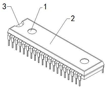
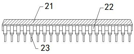
[0029] The present invention provides a multi-chip integrated circuit packaging structure, which structure includes a fixing hole 1, an integrated circuit board 2, and a card slot 3, the fixing hole 1 is fixed on the upper surface of the integrated circuit board 2, and the integrated circuit board 2 It is an integrated structure with the card slot 3; the integrated circuit board 2 includes an upper joint surface 21, a bottom board 22, and pins 23, and the bottom of the upper joint surface 21 is attached to the upper surface of the bottom board 22, The pins 23 are fixed at the front end of the bottom board 22 .

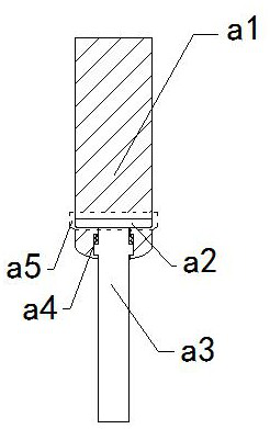
[0030] Wherein, the pin 23 includes an upper board a1, an upper slide a2, a force bar a3, an elastic strip a4, and a collection frame a5, the upper board a1 runs through the inner position of the collection frame a5, and the upper slide a2 The bottom of the upper plate is connected to the top of the force rod a...

Embodiment 2

[0036] For example Figure 6 -example Figure 9 Shown:

[0037] Wherein, the plate surface a24 includes a frame c1, a top sliding rod c2, a sliding plate c3, and a receiving plate c4, the frame c1 is embedded in the inner position of the receiving plate c4, and the top sliding rod c2 is slidingly matched with the inside of the frame c1 , the sliding plate c3 is engaged with the inside of the frame c1, and the rebound force generated by the mechanism shrinking to the extreme can make the top sliding rod c2 slide upwards and protrude along the frame c1 under the cooperation of the sliding plate c3, so that the top The slide bar c2 can be pushed away from the solidified resin block that is not formed into pieces on the receiving plate c4.

[0038] Wherein, the top sliding rod c2 includes a side swing plate c21, a lower fixing plate c22, a pull piece c23, and a middle connecting rod c24, the bottom of the side swing plate c21 is hinged to the bottom of the middle connecting rod c2...


PUM


Abstract

The invention discloses a multi-chip integrated circuit packaging structure which structurally comprises a fixing hole, an integrated circuit board and a clamping groove, the fixing hole is fixed to the position of the upper surface of the integrated circuit board, the integrated circuit board and the clamping groove are of an integrated structure, molten resin flowing downwards along pins can be collected through a collecting frame on the pins, the stress rods can generate upward reverse thrust on the upper sliding plate through reverse thrust generated by the platform on the stress rods on the pins, so that the upper sliding plate can slide upwards along the inner wall of the collecting frame, the upper sliding plate can push out the solidified branch layer in the collecting frame upwards, through collision generated by resetting of the upper sliding plate and the inner wall of the collecting frame, a top sliding rod can upwards slide and extend out along the frame under the cooperation of a sliding plate, so that an upper sliding plate can push up a resin solidification block on the upper surface of the frame, and the situation that an upper push rod cannot easily and effectively remove a resin solidification layer on the upper surface of the upper sliding plate is effectively avoided.

Description

technical field [0001] The invention relates to the technical field of integrated circuit packaging, in particular to a multi-chip integrated circuit packaging structure. Background technique [0002] Multi-chip integrated circuit packaging board is a finished product obtained by packaging integrated circuits of multiple chips. After melting resin and other materials used for integrated circuit packaging and covering them on multi-chip integrated circuits, after the resin is air-dried and solidified, it can The multi-chip integrated circuit packaging board with pins outside is obtained. Based on the above description, the inventors found that the existing multi-chip integrated circuit packaging structure mainly has the following deficiencies, for example: [0003] Since the pins of the multi-chip integrated circuit packaging board are vertically downward, and the resin will flow after melting, if the resin coverage is large, it is easy for the molten resin to flow out to the...

Claims


Application Information

Patent Timeline
IPC IPC(8): H01L25/065H01L23/50
CPCH01L25/065H01L23/50
Inventor 李琴
Owner 深圳市好年华电子有限公司
Learn More