Image sensing device and exposure time adjusting method thereof

A technology of exposure time and image sensing, which is applied in image communication, print image collection, fingerprint/palmprint acquisition/sorting, etc., can solve the problems of exposure time adjustment failure, increased production cost, poor efficiency, etc., to avoid signal The effect of converting errors, improving efficiency, and reducing production costs

Active Publication Date: 2021-07-23
EGIS TECH
View PDF7 Cites 0 Cited by
  • Summary
  • Abstract
  • Description
  • Claims
  • Application Information

AI Technical Summary

Problems solved by technology

Although this method allows the image sensing device to have an appropriate exposure time and provide a clear sensing image, it has the problems of poor efficiency, increased production costs, and errors in the signal conversion process that lead to exposure time adjustments. risk of failure

Method used


Image

  • Image sensing device and exposure time adjusting method thereof
  • Image sensing device and exposure time adjusting method thereof
  • Image sensing device and exposure time adjusting method thereof

Examples


Embodiment Construction

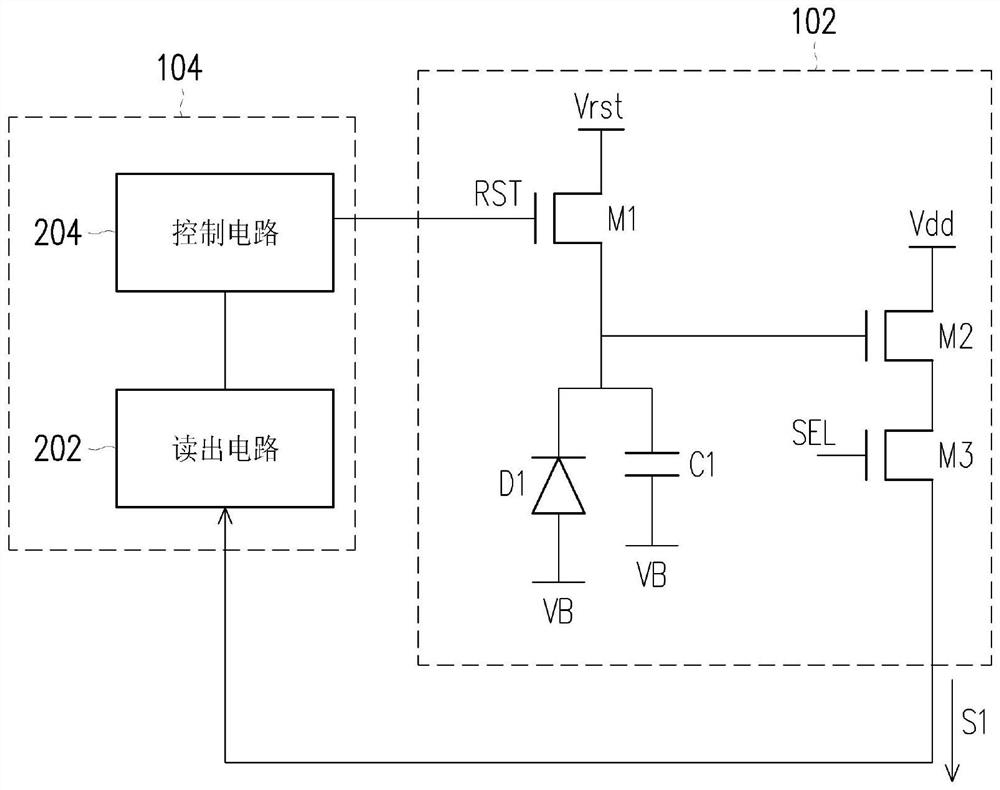
[0012] figure 1 is a schematic diagram of an image sensing device according to an embodiment of the present invention, please refer to figure 1 . The image sensing device may include a light sensing unit 102 and an exposure time adjustment circuit 104 , and the light sensing unit 102 is coupled to the exposure time adjustment circuit 104 . The image sensing device can be, for example, a fingerprint sensor or an X-ray flat panel sensor, but is not limited thereto. The light sensing unit 102 can receive a light signal including image information to generate a sensing signal S1, and the image information can include fingerprint information or palmprint information. The exposure time adjustment circuit 104 is integrated into a chip connected to the light sensing unit 102, such as a fingerprint image reading chip, a fingerprint recognition algorithm chip, etc. limit.

[0013] The exposure time adjustment circuit 104 can adjust the exposure time of the photo-sensing unit 102 acc...


PUM


Abstract

The invention provides an image sensing device and an exposure time adjusting method thereof. A light sensing unit senses a light signal including image information to generate a sensing signal. An exposure time adjusting circuit is integrated in the chip and adjusts the exposure time of the light sensing unit according to the sensing signal.

Description

technical field [0001] The invention relates to a sensing device, in particular to an optical image sensing device and an exposure time adjustment method thereof. Background technique [0002] A common image sensing device may include a sensing pixel array composed of a plurality of sensing pixels, each sensing pixel may convert incident light into a sensing signal, and by analyzing the sensing signal provided by each sensing pixel, that is The image sensed by the sensing pixel array can be obtained. Further, each sensing pixel may include a photodiode, which can convert light into an electrical signal. The continuous exposure of the photodiode will cause the voltage value of the sensing signal output by the sensing pixel to continuously decrease. By reading the sensing signal The image sensed by each sensing pixel can be obtained. However, when the exposure amount is too small (for example, the exposure time is too short), that is, the voltage value of the sensing signal ...

Claims


Application Information

Patent Timeline
Patent Type & Authority Applications(China)
IPC IPC(8): H04N5/225H04N5/235
CPCH04N23/50H04N23/71H04N23/73G06V10/147G06V40/1318
Inventor 罗婉榕
Owner EGIS TECH
Why Eureka
Try Eureka