Electro-optical crystal film for electro-optical modulator, preparation method and electronic component
A technology of electro-optical modulator and electro-optical crystal, which is applied in the manufacture of electrical components, optical components, semiconductor/solid-state devices, etc.
- Summary
- Abstract
- Description
- Claims
- Application Information
AI Technical Summary
Problems solved by technology
Method used
Image
Examples
Example Embodiment
[0034] The following will clearly and completely describe the technical solutions in the embodiments of the application with reference to the drawings in the embodiments of the application. Apparently, the described embodiments are only some of the embodiments of the application, not all of them. Based on the embodiments in this application, all other embodiments obtained by those skilled in the art without making creative efforts belong to the scope of protection of this application.
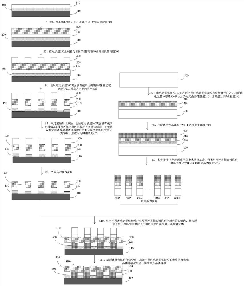
[0035] see figure 1 , the application provides a method for preparing an electro-optic crystal film for an electro-optic modulator, comprising the following steps:
[0036] Step 1. Prepare an SOI substrate, which includes a substrate layer 110 , an oxide layer 120 and a silicon layer 130 sequentially stacked from bottom to top.
[0037] SOI (Silicon-On-Insulator, silicon on insulating substrate), introduces a buried oxide layer between the top silicon layer and the substrate layer. By forming...
PUM
| Property | Measurement | Unit |
|---|---|---|
| Length | aaaaa | aaaaa |
| Width | aaaaa | aaaaa |
Abstract
Description
Claims
Application Information
 - R&D
- Intellectual Property
- Life Sciences
- Materials
- Tech Scout
- Unparalleled Data Quality
- Higher Quality Content
- 60% Fewer Hallucinations
Browse by: Latest US Patents, China's latest patents, Technical Efficacy Thesaurus, Application Domain, Technology Topic, Popular Technical Reports.
© 2025 PatSnap. All rights reserved.Legal|Privacy policy|Modern Slavery Act Transparency Statement|Sitemap|About US| Contact US: help@patsnap.com


