
Semiconductor process chamber and semiconductor process equipment

A technology of process chamber and process equipment, applied in semiconductor/solid-state device manufacturing, electrical components, circuits, etc., can solve the problem of uneven direction and speed of gas movement, unstable stoichiometric specific resistivity, affecting the uniform thickness of the deposited film It can improve the unevenness of airflow, improve the uniformity and stability of nitride resistivity, and enhance the process capability of the equipment.

Active Publication Date: 2021-09-17
BEIJING NAURA MICROELECTRONICS EQUIP CO LTD
View PDF13 Cites 0 Cited by
  • Summary
  • Abstract
  • Description
  • Claims
  • Application Information

AI Technical Summary

Problems solved by technology

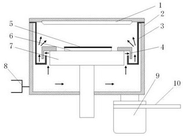
The air flow in the cavity enters the cavity 2 from the air inlet 8, and enters the process area above the base 7 through the bent air flow channel between the lining 3 and the snap ring 4, and the base 7 is close to the two sides of the air inlet 8 and the cold pump 9. There are different gas flows on the side, resulting in uneven direction and speed of gas movement in the process area above the susceptor 7, thereby affecting the uniformity of the deposited film thickness, and the stoichiometric ratio of metal and nitrogen in the metal nitride film is easily affected by cooling The resistivity is unstable due to the influence of the pumping speed change
In addition, limited by the current chamber structure and air intake method, a large amount of Ar / N enters the chamber 2 and is directly pumped away by the cold pump 9, and only a small amount of process gas passes through the bend between the lining 3 and the snap ring 4. The folded air flow channel enters the process area above the base 7, and the process cost is relatively high

Method used


Image

  • Semiconductor process chamber and semiconductor process equipment
  • Semiconductor process chamber and semiconductor process equipment
  • Semiconductor process chamber and semiconductor process equipment

Examples


Embodiment Construction

[0027] Embodiments of the present invention are described in detail below, examples of which are shown in the drawings, wherein the same or similar reference numerals designate the same or similar elements or elements having the same or similar functions throughout. The embodiments described below by referring to the figures are exemplary only for explaining the present invention and should not be construed as limiting the present invention.

[0028] In describing the present invention, it should be understood that the terms "center", "longitudinal", "transverse", "length", "width", "thickness", "upper", "lower", "front", " Back", "Left", "Right", "Vertical", "Horizontal", "Top", "Bottom", "Inner", "Outer", "Clockwise", "Counterclockwise", "Axial" , "radial", "circumferential" and other indicated orientations or positional relationships are based on the orientations or positional relationships shown in the drawings, which are only for the convenience of describing the present ...


PUM


Abstract

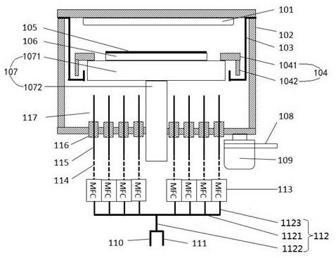
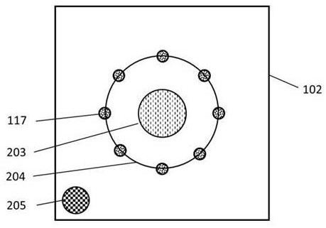
The present invention provides a process chamber in semiconductor process equipment and semiconductor process equipment, wherein, the process chamber includes a chamber body, an air inlet device, and a base arranged inside the chamber body, and the process chamber The gas device includes a plurality of air intake pipelines, which are arranged around the base and are all located under the base, and each of the air intake pipelines is provided with a flow control mechanism. In the present invention, by designing an air intake device, the process gas can be more accurately controlled and dispersed in the process chamber, and the gas movement in the process area is more uniform, thereby eliminating the influence of the cold pump bias on the air flow movement in the process chamber, thereby achieving The purpose of improving the uniformity of deposited film, enhancing the process capability of equipment and improving product quality.

Description

technical field [0001] The invention relates to the technical field of semiconductor manufacturing, in particular to a process chamber in semiconductor process equipment and semiconductor process equipment. Background technique [0002] In the research of integrated circuits, the use of copper instead of aluminum as the leads of integrated circuits has attracted widespread attention in the industry. In order to prevent copper from diffusing in silicon and silicon oxides and reacting with silicon, an anti-diffusion layer is usually added between copper and the circuit. Metal nitrides (such as TaN / TiN) have excellent thermal stability, good electrical conductivity, high melting point, and high lattice and grain boundary stability, so they have become the material of choice for the anti-diffusion layer. [0003] The use of PVD magnetron sputtering to deposit metal nitride films (such as TaN / TiN) has many advantages: simple process, good repeatability, and a film with a high cr...

Claims


Application Information

Patent Timeline
Patent Type & Authority Patents(China)
IPC IPC(8): H01L21/67
CPCH01L21/67253
Inventor 黄其伟
Owner BEIJING NAURA MICROELECTRONICS EQUIP CO LTD
Learn More