A high-performance large-area flexible transparent electrode and its preparation method and application
A transparent electrode, large-area technology, used in cable/conductor manufacturing, circuits, electrical components, etc., can solve the problems of limited transfer materials, difficult demolding, expensive equipment, etc., to achieve low process costs and simple process steps. , the effect of low manufacturing capacity
- Summary
- Abstract
- Description
- Claims
- Application Information
AI Technical Summary
Problems solved by technology
Method used
Image
Examples
Embodiment 1
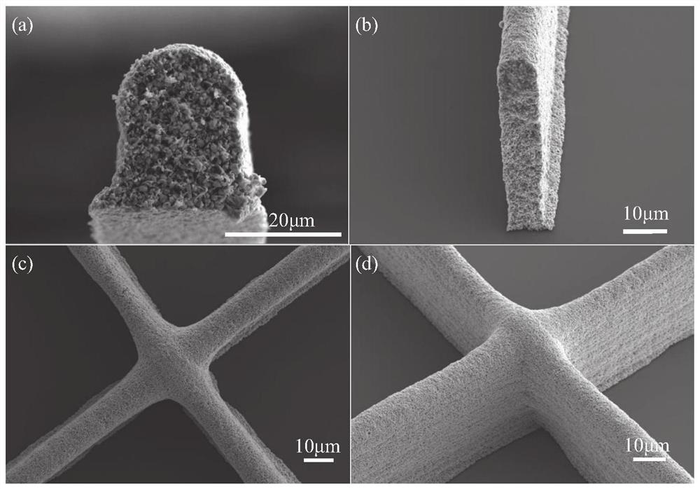
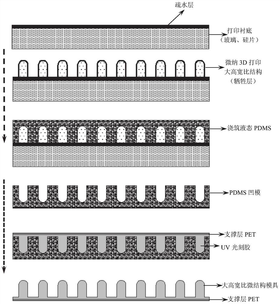
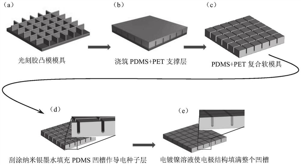
[0057] In this example, nano-conductive silver paste (NT-ST20E) is used as the printing material. First, the electric field-driven jet micro-nano 3D printing technology is used to print an ultra-fine, high-aspect-ratio wire grid structure as a sacrifice by multi-layer printing. Then, the corresponding PDMS concave mold structure is transferred on the sacrificial layer structure; then, using UV photoresist as the transfer material, the corresponding convex mold structure is transferred as the master mold , and transfer the structure on the master mold to the PDMS-PET composite mold to form a soft mold with ultra-fine and large aspect ratio; finally, the electrode structure is filled with the entire groove by electroplating process, and further conductive treatment is performed. An embedded, high-performance flexible transparent conductive film is obtained.
[0058] The process steps of manufacturing an ultra-fine, large-aspect-ratio embedded flexible transparent conductive film...
Embodiment 2
[0079] In this example, nano-conductive silver paste (NT-ST20E) is used as the printing material. First, the electric field-driven jet micro-nano 3D printing technology is used to print an ultra-fine, high-aspect-ratio grid structure as a sacrifice by multi-layer printing. Then, the corresponding PDMS concave mold structure is transferred on the sacrificial layer structure; then, using UV photoresist as the transfer material, the corresponding convex mold structure is transferred as the master mold , and transfer the structure on the master mold to the PDMS-PET composite mold to form a soft mold with ultra-fine and large aspect ratio; finally, the electrode structure is filled with the entire groove by electroplating process, and further conductive treatment is performed. An embedded, high-performance flexible transparent conductive film is obtained.
[0080] The process steps of manufacturing an ultra-fine, large-aspect-ratio embedded flexible transparent conductive film in t...
PUM
| Property | Measurement | Unit |
|---|---|---|
| thickness | aaaaa | aaaaa |
| width | aaaaa | aaaaa |
| thickness | aaaaa | aaaaa |
Abstract
Description
Claims
Application Information
 - R&D Engineer
- R&D Manager
- IP Professional
- Industry Leading Data Capabilities
- Powerful AI technology
- Patent DNA Extraction
Browse by: Latest US Patents, China's latest patents, Technical Efficacy Thesaurus, Application Domain, Technology Topic, Popular Technical Reports.
© 2024 PatSnap. All rights reserved.Legal|Privacy policy|Modern Slavery Act Transparency Statement|Sitemap|About US| Contact US: help@patsnap.com


