
Image sensor

A technology of image sensors and photosensitive elements, applied in the field of image sensors, can solve problems such as poor image quality, achieve the best image quality, reduce dark current, and prevent stray light interference

Pending Publication Date: 2021-03-19
POWERCHIP SEMICON MFG CORP
View PDF0 Cites 0 Cited by
  • Summary
  • Abstract
  • Description
  • Claims
  • Application Information

AI Technical Summary

Problems solved by technology

However, the interference (crosstalk) caused by stray light to the signal stored in the storage node and the dark current (dark current) generated by interface defects will cause poor image quality

Method used


Image

  • Image sensor
  • Image sensor
  • Image sensor

Examples


Embodiment Construction

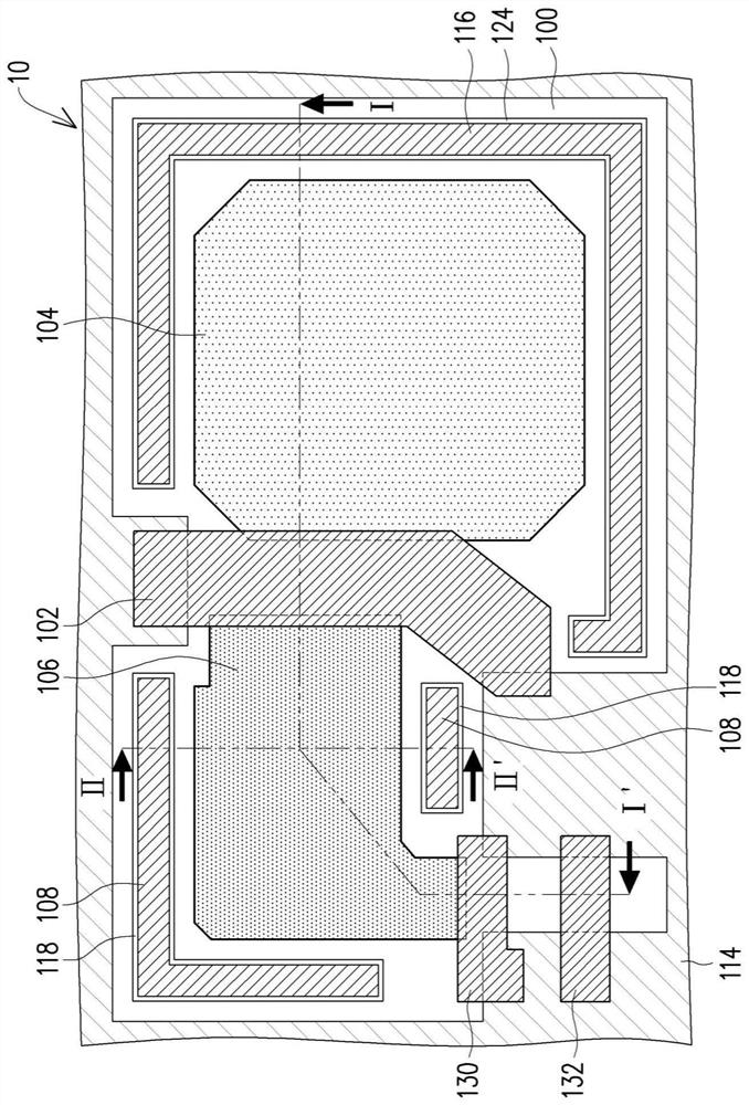
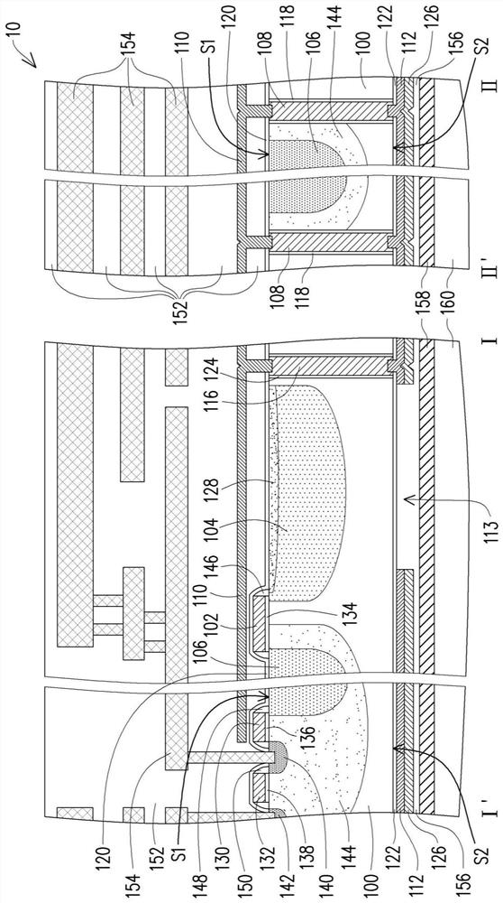
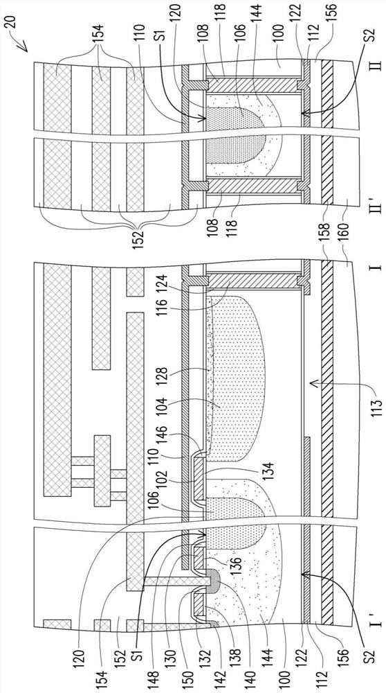
[0042] figure 1 It is a top view of an image sensor according to an embodiment of the present invention. figure 2 for along figure 1 The cross-sectional view of the I-I' section line and the II-II' section line in the figure. exist figure 1 omitted figure 2 Some of the components in are clearly drawn figure 1 The configuration relationship between the components in .

[0043] Please refer to figure 1 and figure 2 , the image sensor 10 includes a substrate 100 , a gate 102 , a photosensitive element 104 , a storage node 106 , at least one reflective layer 108 , a reflective layer 110 and a reflective layer 112 . In this embodiment, the image sensor 10 is an example of a back-illuminated image sensor, but the present invention is not limited thereto.

[0044] The substrate 100 has a first surface S1 and a second surface S2 opposite to each other. The material of the substrate 100 is, for example, semiconductor material, such as epitaxial silicon, but the present inve...


PUM


Abstract

The invention discloses an image sensor. The image sensor comprises a substrate, a first grid, a photosensitive element, a storage node, at least one first reflective layer, a second reflective layerand a third reflective layer. The substrate has a first surface and a second surface opposite to each other. The first grid is disposed on the substrate of the first side. The photosensitive element is located in the substrate on one side of the first grid. The storage node is located in the substrate on the other side of the first grid. The first reflective layer is disposed in the substrate andlocated around the storage node. The second reflective layer shields the storage node on the first surface and is electrically connected to the first reflective layer. The third reflective layer shields the storage node on the second surface and is electrically connected with the first reflective layer.

Description

technical field [0001] The invention relates to a semiconductor device, and in particular to an image sensor. Background technique [0002] Currently, some types of image sensors (eg, global shutter image sensors) have storage nodes located in the substrate for storing signals. However, the interference (crosstalk) caused by stray light to the signal stored in the storage node and the dark current (dark current) generated by interface defects will cause poor image quality. Therefore, how to effectively prevent stray light interference and reduce dark current is the goal of continuous efforts. Contents of the invention [0003] The invention provides an image sensor, which can effectively prevent stray light interference and reduce dark current. [0004] The present invention provides an image sensor, including a substrate, a first gate, a photosensitive element, a storage node, at least one first reflective layer, a second reflective layer and a third reflective layer. ...

Claims


Application Information

Patent Timeline
Patent Type & Authority Applications(China)
IPC IPC(8): H01L27/146
CPCH01L27/14629H01L27/14623H01L27/14609H01L27/14645
Inventor 钟志平何明祐毕嘉慧
Owner POWERCHIP SEMICON MFG CORP
Learn More