2D scan tree structure for measurable scan design of low-power integrated circuits
A two-dimensional scanning, integrated circuit technology, applied in the direction of electronic circuit testing, circuits, electrical components, etc., can solve the problems of complex structure and low symmetry, and achieve the effect of large optimization space, reducing requirements and reducing interconnection complexity.
- Summary
- Abstract
- Description
- Claims
- Application Information
AI Technical Summary
Problems solved by technology
Method used
Image

Examples
Embodiment 2
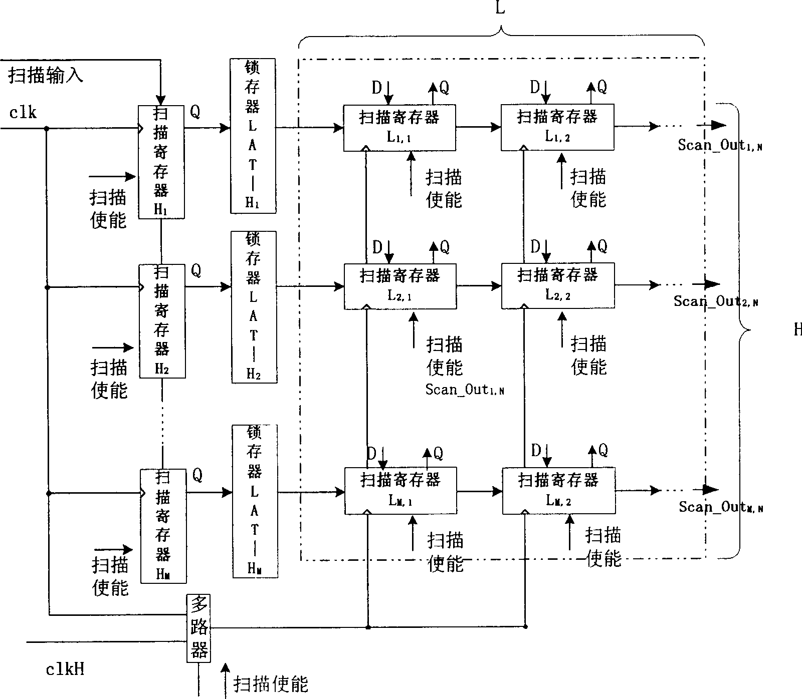
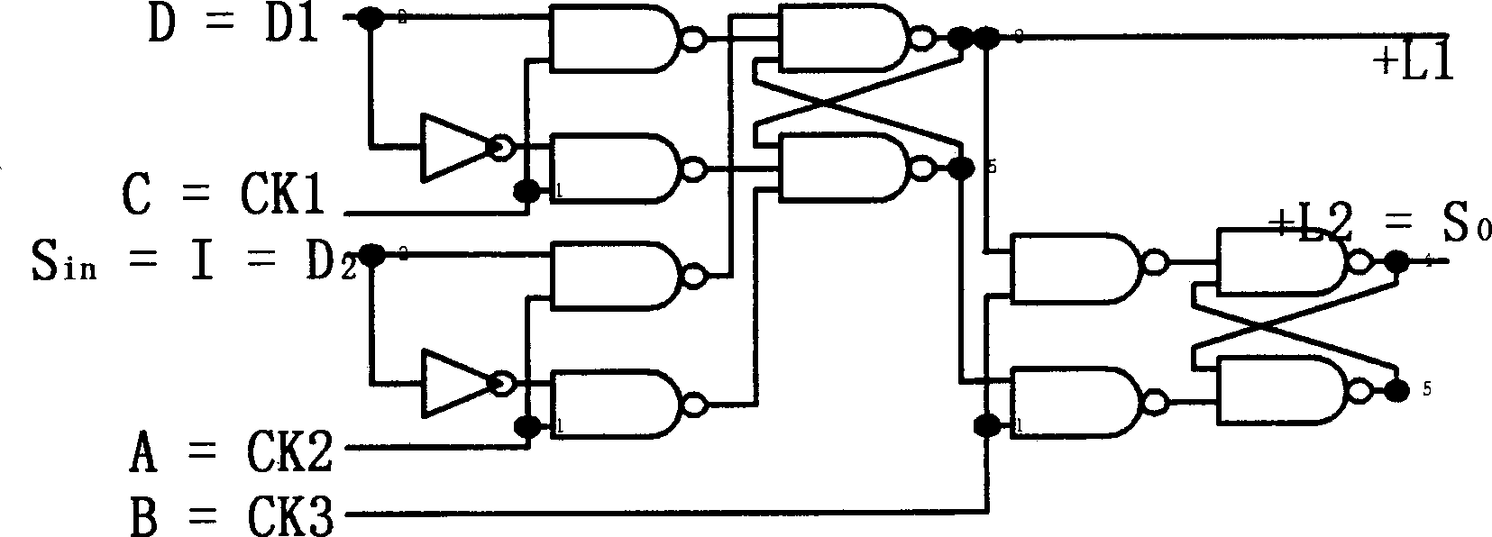
[0035] In the second embodiment, a two-dimensional L×H scan tree structure is formed by 1000 scan register units, wherein L=200, H=5, and the two-dimensional scan tree circuit used by each scan register unit SSF is the same as that in the first embodiment, such as image 3 shown.
Embodiment 3
[0036] In the third embodiment, a two-dimensional L×H scanning tree structure is formed by 5000 scanning register units, wherein L=1000 H=5. The two-dimensional scan tree circuit used by each scan register unit SSF is the same as that in the first embodiment, such as image 3 shown.
[0037] Table 1 shows the comparison of the bit pass rate between the above three embodiments and the traditional one-dimensional scan register structure.
Embodiment 1
[0038] Embodiment 1: The number of scan register units is N=500. If a one-dimensional scan chain is used, the bit pass rate (RBP1)=125250. When H=5, that is, H / N=1%, the bit pass rate (RBP2 )=6550, RBP1 / RBP2=19.12, that is to say, the power consumption of the circuit using the two-dimensional scanning structure is about 1 / 19 of that of the one-dimensional scanning circuit.
[0039] Implementation 2: The number of scan register units is N=1000, if a one-dimensional scan chain is used, its bit pass rate (RBP1)=500500, when H=5, that is to say H / N=0.5%, the bit pass rate (RBP2) =23100, RBP1 / RBP2=21.67, that is to say, the power consumption of the circuit using the two-dimensional scanning structure is about 1 / 21 of that of the one-dimensional scanning circuit.
[0040] Implementation 3: The number of scan register units is N=5000, if a one-dimensional scan chain is used, the bit pass rate (RBP1)=12502500, when H=10, that is to say H / N=0.2%, the bit pass rate (RBP2) =152750, RBP1...
PUM
 Abstract
Description
Claims
Application Information
 - Generate Ideas
- Intellectual Property
- Life Sciences
- Materials
- Tech Scout
- Unparalleled Data Quality
- Higher Quality Content
- 60% Fewer Hallucinations
Browse by: Latest US Patents, China's latest patents, Technical Efficacy Thesaurus, Application Domain, Technology Topic, Popular Technical Reports.
© 2025 PatSnap. All rights reserved.Legal|Privacy policy|Modern Slavery Act Transparency Statement|Sitemap|About US| Contact US: help@patsnap.com