Transient voltage suppression diode structure and manufacturing method thereof

A technology of transient voltage suppression and manufacturing method, applied in diodes, semiconductor/solid-state device manufacturing, circuits, etc., can solve problems such as poor surge current capability, and achieve the effect of reducing size and improving IPP surge current capability

Pending Publication Date: 2020-12-08
WUXI CHINA RESOURCES HUAJING MICROELECTRONICS
View PDF5 Cites 3 Cited by
  • Summary
  • Abstract
  • Description
  • Claims
  • Application Information

AI Technical Summary

Problems solved by technology

[0005] However, existing TVS diode devices are resistant to I PP Relatively poor surge current capability

Method used


Image

  • Transient voltage suppression diode structure and manufacturing method thereof
  • Transient voltage suppression diode structure and manufacturing method thereof
  • Transient voltage suppression diode structure and manufacturing method thereof

Examples


Embodiment Construction

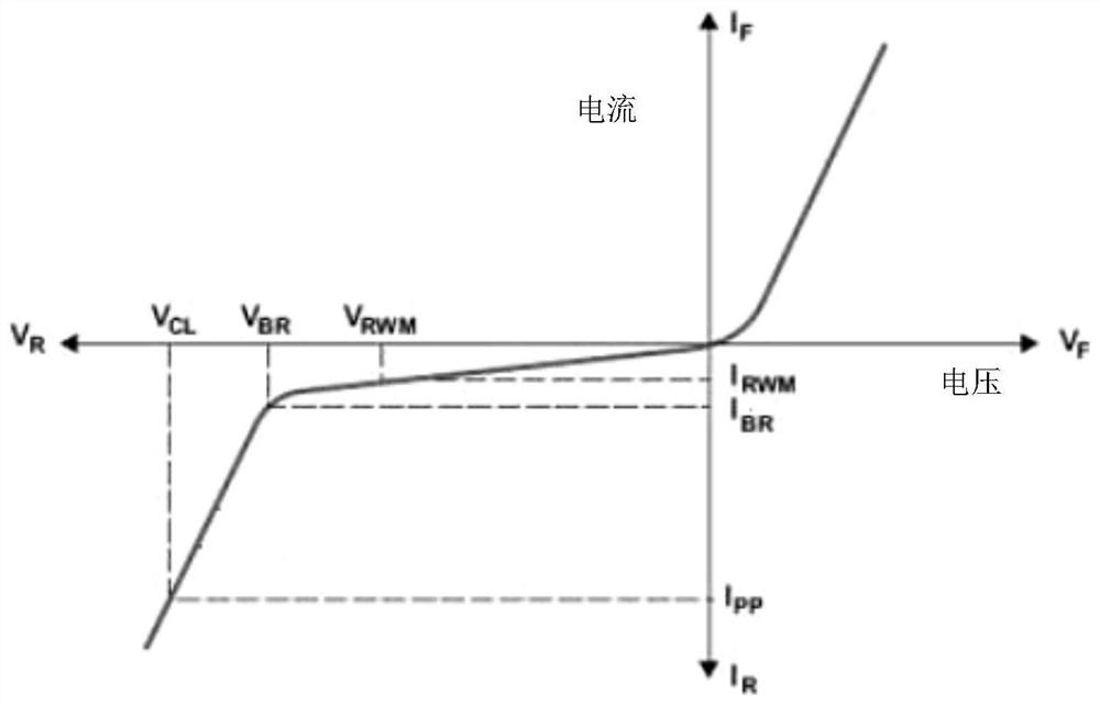
[0049] The inventor researched and analyzed the reverse use process of the unidirectional transient voltage suppression diode, and found that most of the I PPThe surge current flows from the N-type layer to the P-type layer at the corners of the PN junction. This causes the current density in the middle and corners of the PN junction to be unequal, causing anti-I PP The surge current capability is relatively poor.

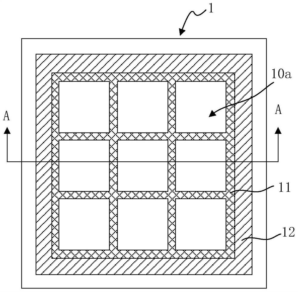
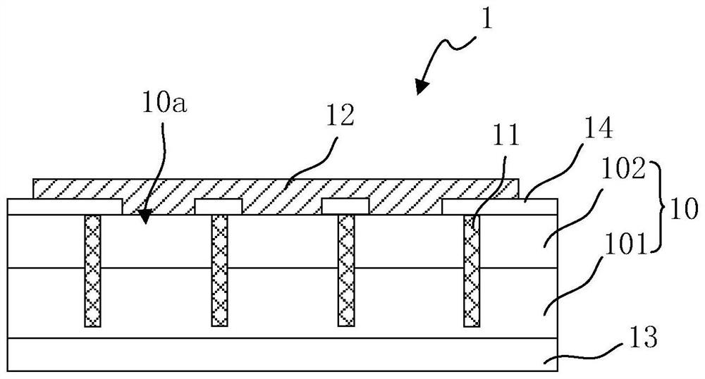
[0050] Based on the above analysis, the present invention proposes: a plurality of isolation rings are arranged in the semiconductor stack, and the semiconductor stack is separated into a plurality of stack units by the plurality of isolation rings; the first electrode and the second electrode are respectively formed on the upper surface and the lower surface of the semiconductor stack. Two electrodes, the first electrode and the second electrode are continuously distributed in each lamination unit. In other words, each stack unit corresponds to a transient volta...


PUM

PropertyMeasurementUnit
electrical resistivityaaaaaaaaaa
thicknessaaaaaaaaaa

Abstract

The invention provides a transient voltage suppression diode structure and a manufacturing method thereof, and the structure is characterized in that a plurality of isolation rings are disposed in a semiconductor lamination layer, and divide the semiconductor lamination layer into a plurality of lamination units; and a first electrode and a second electrode are correspondingly formed on the uppersurface and the lower surface of the semiconductor lamination respectively, wherein the first electrode and the second electrode are continuously distributed in each lamination unit. In other words, each lamination unit corresponds to one transient voltage suppression sub-diode, and the transient voltage suppression sub-diodes are connected in parallel. When the transient voltage suppression diodes are used reversely, due to the fact that the transient voltage suppression sub-diodes are connected in parallel, flow channels for IPP surge currents can be provided for all the lamination units, specifically, the positions, close to the isolation ring, of all the lamination units, and the IPP surge currents in all the flow channels are reduced. Therefore, the IPP surge current resistance of thetransient voltage suppressor diode device is improved.

Description

technical field [0001] The invention relates to the technical field of semiconductor devices, in particular to a transient voltage suppression diode structure and a manufacturing method thereof. Background technique [0002] Transient Voltage Suppressor (TVS), when the two poles are subjected to a reverse transient high-energy impact, can effectively protect the precision components in the electronic circuit from damage by various surge pulses. [0003] figure 1 is the volt-ampere characteristic curve of a unidirectional transient voltage suppressor diode. refer to figure 1 As shown, when the transient voltage suppression diode is used in the forward direction, the forward conduction current I F vs. forward voltage V F The volt-ampere curve between them is the same as that of ordinary diodes. [0004] still refer to figure 1 As shown, when the transient voltage suppression diode is used in reverse, the reverse conduction current I R with reverse voltage V R The relat...

Claims


Application Information

Patent Timeline
Patent Type & Authority Applications(China)
IPC IPC(8): H01L29/06H01L29/861H01L21/329H01L27/02
CPCH01L29/8613H01L29/66136H01L29/0619H01L29/0696H01L29/0649H01L27/0255H01L27/0296
Inventor 吴志伟毛虹懿
Owner WUXI CHINA RESOURCES HUAJING MICROELECTRONICS
Why Eureka
Try Eureka