Wafer bonding machine clamp for semiconductor light-emitting display

A technology for light-emitting displays and die bonders, which is applied in the fields of semiconductor devices, semiconductor/solid-state device manufacturing, electrical components, etc.

Inactive Publication Date: 2020-07-07
漳州市杰成电子产品有限公司
View PDF7 Cites 0 Cited by
  • Summary
  • Abstract
  • Description
  • Claims
  • Application Information

AI Technical Summary

Problems solved by technology

[0003] The purpose of the present invention is to provide a semiconductor light-emitting display die-bonding machine fixture to solve the problem that the existing die-bonding machine fixture proposed in the above-mentioned background technology cannot be used for products due to long-term wear and tear. It is fixed to make it slide down, which affects the processing level, and the existing fixture of a die-bonding machine, because impurities or other industrial waste will fall into the chute during processing, the fixture cannot be moved, which not only increases the The user's use burden also reduces the problem of the user's work efficiency. Therefore, we propose a semiconductor light-emitting display die-bonding machine fixture.

Method used


Image

  • Wafer bonding machine clamp for semiconductor light-emitting display
  • Wafer bonding machine clamp for semiconductor light-emitting display
  • Wafer bonding machine clamp for semiconductor light-emitting display

Examples


Embodiment Construction

[0020] The following will clearly and completely describe the technical solutions in the embodiments of the present invention with reference to the accompanying drawings in the embodiments of the present invention. Obviously, the described embodiments are only some of the embodiments of the present invention, not all of them. Based on the embodiments of the present invention, all other embodiments obtained by persons of ordinary skill in the art without making creative efforts belong to the protection scope of the present invention.

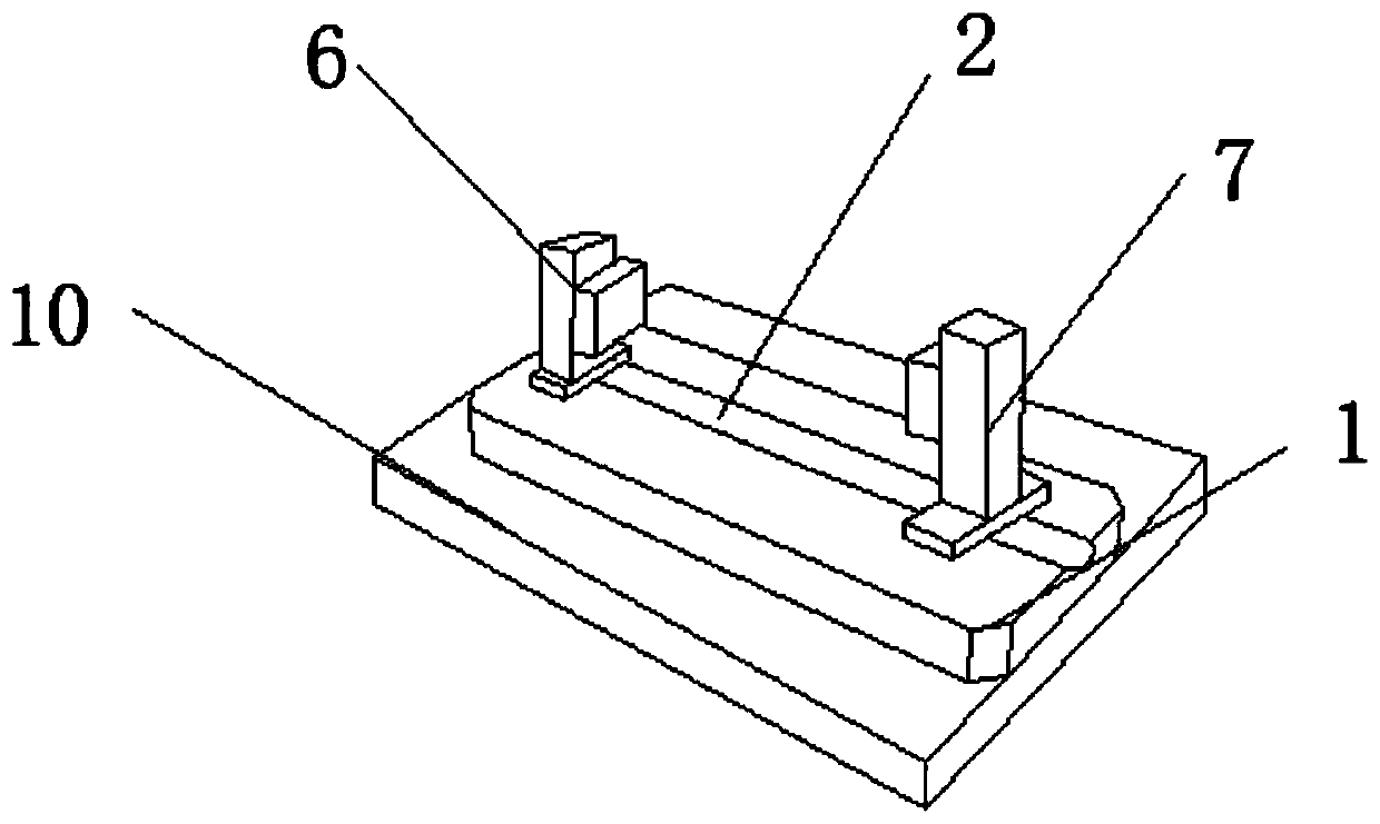
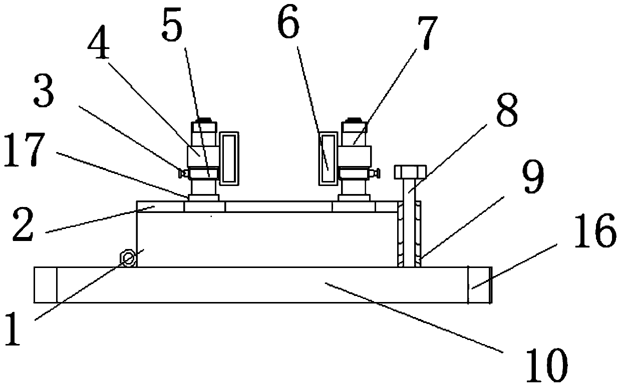
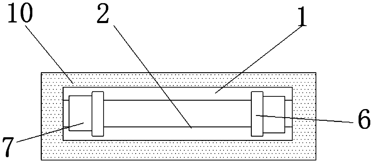
[0021] see Figure 1-Figure 5 , the present invention provides a technical solution: a semiconductor light-emitting display die-bonding machine fixture, including a backing plate 1, one end of the backing plate 1 is provided with a threaded hole 9, the backing plate 1 is movably connected with a bolt 8 through the threaded hole 9, and the bolt 8 runs through the inside of the backing plate 1, and the upper surface of the backing plate 1 is provid...


PUM


Abstract

The invention discloses a wafer bonding machine clamp for a semiconductor light-emitting display. The clamp includes a base plate, wherein a threaded hole is formed in one end of the base plate; the base plate is movably connected with a bolt through the threaded hole; the bolts penetrate through the interiors of the base plates; a sliding groove is formed in the surface of the upper end of the base plate. The two ends of the base plate are movably connected with connecting plates through sliding grooves. A rotating shaft is fixedly connected to the interior of the connecting plate, a fixing rod is fixedly connected to one end of the rotating shaft, a supporting rod is movably connected to one end of the connecting plate, a connecting sleeve is movably connected to the middle of the outersurface of the supporting rod, and a clamping plate is fixedly connected to one end of the connecting sleeve. In the invention, by designing the sliding groove formed in the outer surface of the clamping plate and the limiting plates at the two ends of the clamping plate, a workpiece is more stable in the machining process, and the situation that the machining level is affected due to the fact that the workpiece falls off from the limiting plates during machining is avoided.

Description

technical field [0001] The invention belongs to the technical field of crystal-bonding machine fixtures, and in particular relates to a semiconductor light-emitting display crystal-bonding machine fixture. Background technique [0002] An existing fixture of a crystal bonding machine, due to long-term wear and tear during use, can not fix the product, causing it to slip, which affects the processing level, and the existing fixture of a crystal bonding machine, due to the During processing, there will be impurities or other industrial waste falling into the chute, which will cause the fixture to be unable to move, which not only increases the burden on the user, but also reduces the work efficiency of the user. For this reason, we propose a semiconductor Luminous display die bonding machine fixture. Contents of the invention [0003] The purpose of the present invention is to provide a semiconductor light-emitting display die-bonding machine fixture to solve the problem th...

Claims


Application Information

Patent Timeline
Patent Type & Authority Applications(China)
IPC IPC(8): H01L21/67H01L21/687H01L33/48
CPCH01L21/67092H01L33/48H01L21/68721
Inventor 蔡天佑
Owner 漳州市杰成电子产品有限公司
Why Eureka
Try Eureka