Display device and method of manufacturing the same
A display device and display area technology, which is applied in the direction of identification devices, instruments, semiconductor devices, etc., can solve problems such as wiring breakage, and achieve the effect of reducing the cone angle
- Summary
- Abstract
- Description
- Claims
- Application Information
AI Technical Summary
Problems solved by technology
Method used
Image

Examples
no. 1 approach 》
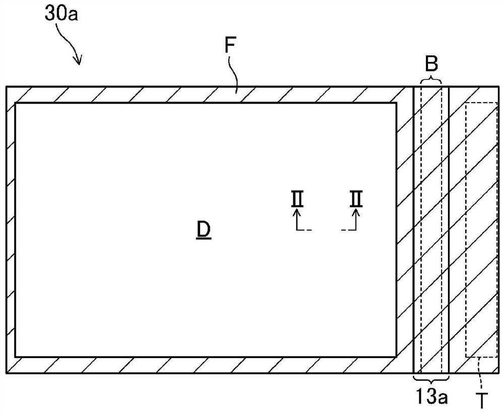
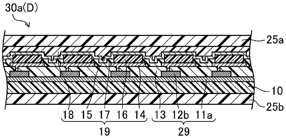
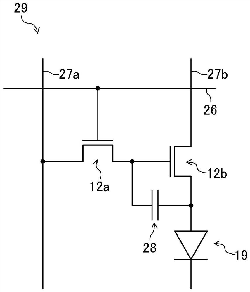
[0030] Figure 1 to Figure 10 The first embodiment of the display device of the present invention is shown. In addition, in each of the following embodiments, an organic EL display device including an organic EL element is exemplified as a display device including a light emitting element. here, figure 1 It is a plan view showing the schematic structure of the organic EL display device 30a of this embodiment. in addition, figure 2 is to mean along figure 1 A cross-sectional view of a schematic structure of a display region D of the organic EL display device 30 a taken along the line II-II in FIG. in addition, image 3 It is an equivalent circuit diagram showing the TFT layer 29 constituting the organic EL display device 30a. in addition, Figure 4 It is a cross-sectional view showing the organic EL layer 16 constituting the organic EL display device 30a. in addition, Figure 5 It is a plan view showing the bent portion B of the frame region F of the organic EL displa...
no. 2 approach 》
[0071] Figure 11 and Figure 12 A second embodiment of the display device of the present invention is shown. here, Figure 11 It is a cross-sectional view showing a schematic structure of the frame region F of the organic EL display device 30b of this embodiment, and is equivalent to Image 6 diagram. in addition, Figure 12 The end portion of the inorganic insulating film L constituting the organic EL display device 30b is enlarged. Figure 11 A detailed cross-sectional view of , and is equivalent to Figure 7 diagram. Furthermore, in each of the following embodiments, for the Figure 1 to Figure 10 The same reference numerals are assigned to the same parts, and detailed description thereof will be omitted.
[0072] In the above-mentioned first embodiment, the organic EL display device 30a manufactured by collectively dry-etching the laminated film of the inorganic insulating film was exemplified, but in this embodiment, the organic EL display device 30a manufactured b...
no. 3 approach 》
[0086] Figure 13 A third embodiment of the display device of the present invention is shown. here, Figure 13 It is a cross-sectional view showing a schematic structure of the frame region F of the organic EL display device 30c of this embodiment, and is equivalent to Image 6 diagram.
[0087] In the above-mentioned first and second embodiments, the organic EL display devices 30a and 30b in which the frame wirings 12ea and 12eb are directly formed on the surface of the resin substrate layer 10 were exemplified. On the surface of the layer 10 , an organic EL display device 30 c is formed with a frame wiring 12 ec via a frame planarizing film 21 .
[0088] The organic EL display device 30c includes a display area D and a frame area F defined around the display area D, similarly to the organic EL display device 30a of the first embodiment.
[0089] The structure of the display region D of the organic EL display device 30c is the same as that of the organic EL display device...
PUM
| Property | Measurement | Unit |
|---|---|---|
| thickness | aaaaa | aaaaa |
| thickness | aaaaa | aaaaa |
| thickness | aaaaa | aaaaa |
Abstract
Description
Claims
Application Information
 - R&D
- Intellectual Property
- Life Sciences
- Materials
- Tech Scout
- Unparalleled Data Quality
- Higher Quality Content
- 60% Fewer Hallucinations
Browse by: Latest US Patents, China's latest patents, Technical Efficacy Thesaurus, Application Domain, Technology Topic, Popular Technical Reports.
© 2025 PatSnap. All rights reserved.Legal|Privacy policy|Modern Slavery Act Transparency Statement|Sitemap|About US| Contact US: help@patsnap.com