Variable inductance device
An Inductive Device, Variable Technology
- Summary
- Abstract
- Description
- Claims
- Application Information
AI Technical Summary
Problems solved by technology
Method used
Image
Examples
Embodiment Construction
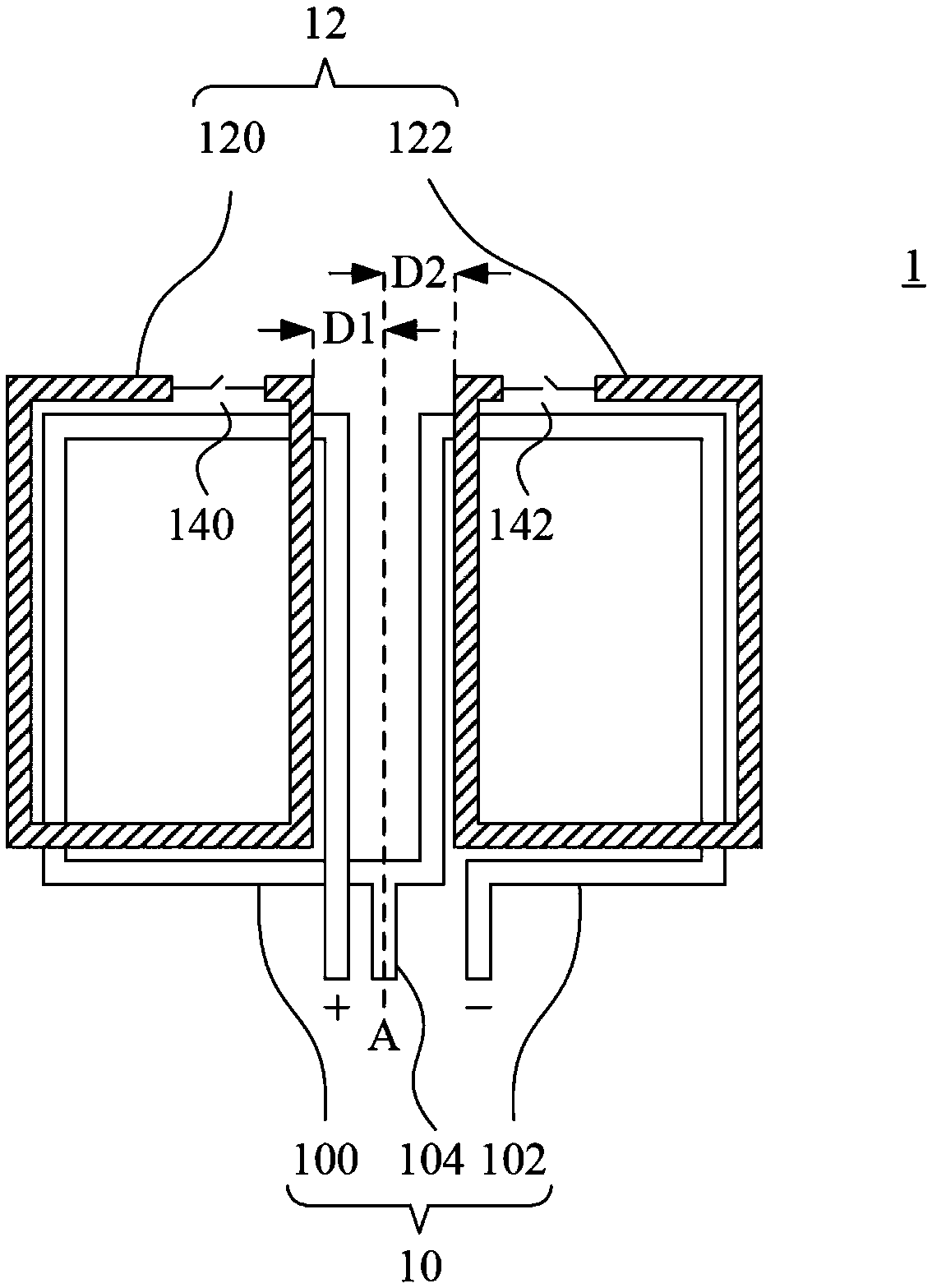
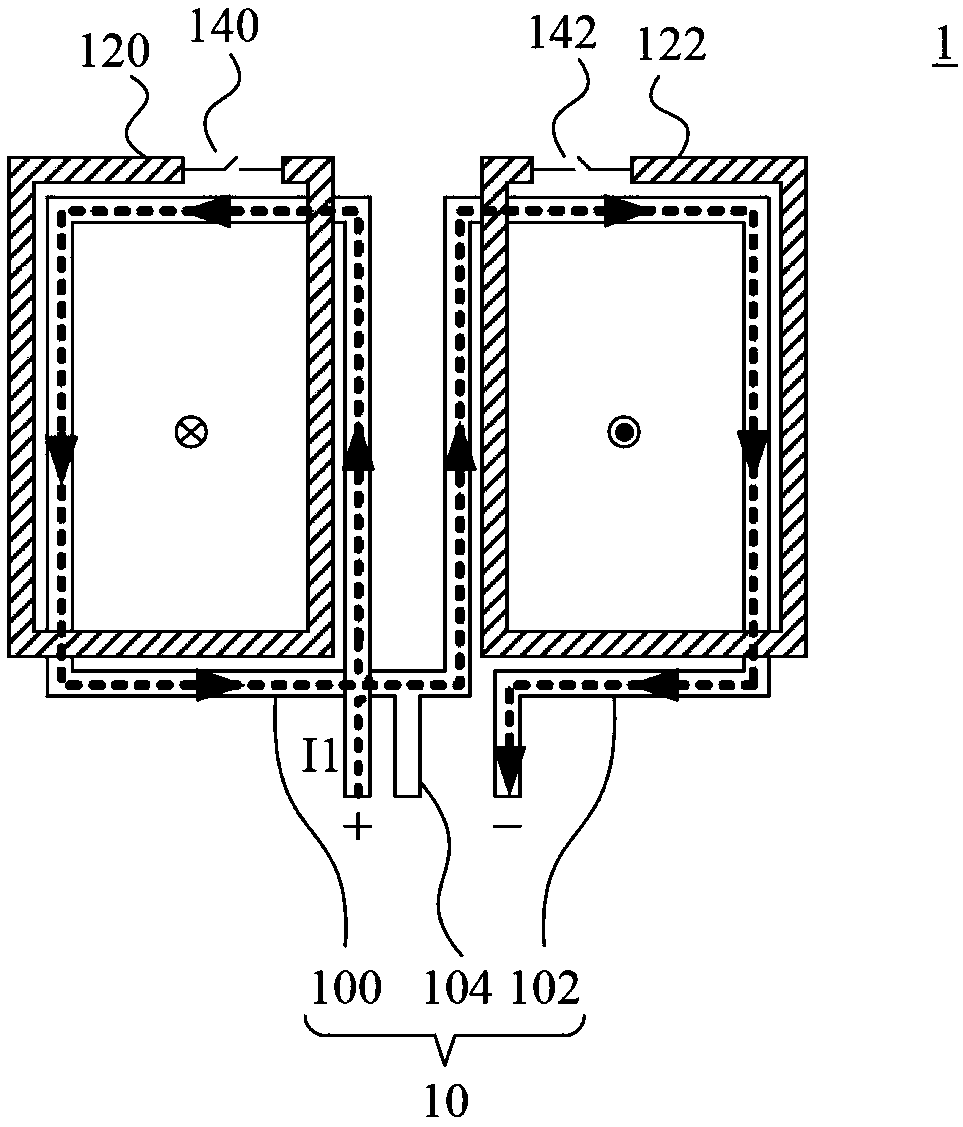
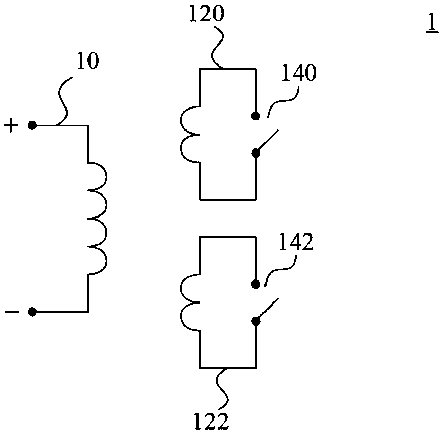
[0048] Please refer to figure 1 . figure 1 It is a schematic diagram of a variable inductance device 1 in an embodiment of the present invention. The variable inductance device 1 includes: a figure-eight inductor 10 , a pair of modulating coils 12 , a first switch 140 and a second switch 142 .
[0049] The figure-eight inductor 10 includes two sub-loops 100 and 102 electrically coupled to each other. Wherein, one end of the sub-loop 100 is electrically coupled to the sub-loop 102, and the other end is electrically coupled to the positive terminal (in figure 1 is represented by the symbol "+"). One end of the sub-loop 102 is electrically coupled to the sub-loop 100, and the other end is electrically coupled to the negative terminal (in figure 1 is represented by the symbol "-").
[0050] In one embodiment, the figure eight inductor 10 further includes a center tap 104 . The center tap 104 is formed on one of the sub-loop 100 and the sub-loop 102 . At figure 1 , the cent...
PUM
 Abstract
Description
Claims
Application Information
 - R&D
- Intellectual Property
- Life Sciences
- Materials
- Tech Scout
- Unparalleled Data Quality
- Higher Quality Content
- 60% Fewer Hallucinations
Browse by: Latest US Patents, China's latest patents, Technical Efficacy Thesaurus, Application Domain, Technology Topic, Popular Technical Reports.
© 2025 PatSnap. All rights reserved.Legal|Privacy policy|Modern Slavery Act Transparency Statement|Sitemap|About US| Contact US: help@patsnap.com


