
Semiconductor molding compound feeding device and working method thereof

A material guide device and molding compound technology, which is applied in semiconductor/solid-state device manufacturing, electrical components, circuits, etc., and can solve problems such as inaccurate position of the molding compound

Pending Publication Date: 2019-12-20
SICHUAN HONGXINWEI TECH
View PDF0 Cites 3 Cited by
  • Summary
  • Abstract
  • Description
  • Claims
  • Application Information

AI Technical Summary

Problems solved by technology

[0005] The purpose of the present invention is to provide a semi-conductor molding compound feeding device, which can solve the current problem of inaccurate position of the molding compound during feeding

Method used


Image

  • Semiconductor molding compound feeding device and working method thereof
  • Semiconductor molding compound feeding device and working method thereof
  • Semiconductor molding compound feeding device and working method thereof

Examples


Embodiment 1

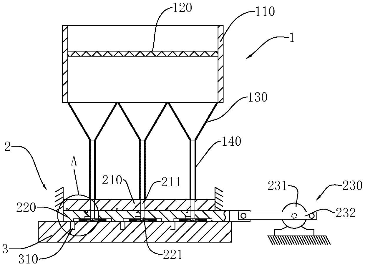
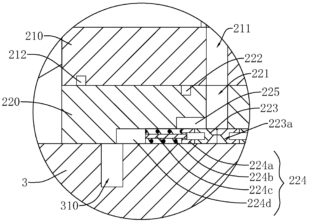
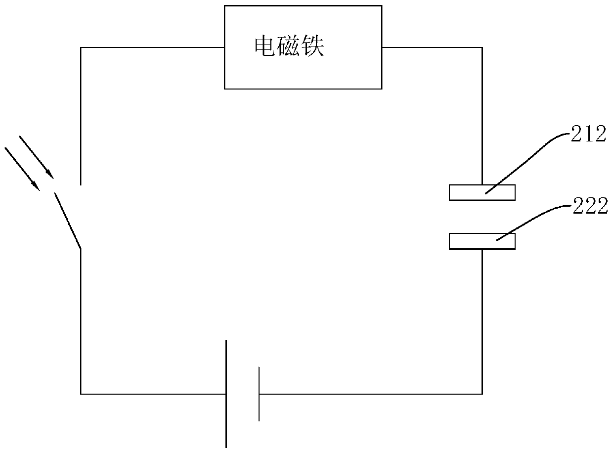
[0032] Embodiment 1, with reference to Figure 1-Figure 4, a semiconductor molding compound feeding device, including a distributing device 1, the distributing device 1 includes a hopper 110, a vibrating screen 120 arranged in the hopper 110, a funnel-shaped feeding device arranged below the vibrating screen 120 The hole 130 and the feeding pipe 140 communicated with the feeding hole 130 are characterized in that they also include a precise material guide device 2, and the precise material guide device 2 includes a horizontally placed upper material guide plate 210, and an upper material guide plate located on the upper material guide plate. 210 below the lower material guide plate 220, the upper material guide plate 210 is provided with a material receiving hole 211 facing the feeding pipe 140, and the lower material guide plate 220 is provided with a height corresponding to the material receiving hole 211 and The blanking hole 221 with the same thickness of the molding compo...

Embodiment 2

[0034] Embodiment two, refer to Figure 5-Figure 7 The upper material guide plate 210 is provided with a blanking hole 213, and a blanking device 228 is arranged in the blanking hole 213. The blanking device 228 includes a vacuum suction cup 228c, and a vacuum pump 228b is connected above the vacuum suction cup 228c. The top of the vacuum pump 228b drives the driving cylinder 228a that the vacuum chuck 228c moves up and down. The inner wall of the blanking hole 221 is provided with a photoelectric sensor 229. The control system is a controller, and the input terminal of the controller communicates with the photoelectric sensor 229 signal. The output ends of the controller are respectively connected with the driving mechanism 230, the power mechanism 224, the driving cylinder 228a and the vacuum chuck 228c. The power mechanism 224 is a discharge cylinder 224e, the drive mechanism 230 is a power cylinder 233, and the rest of the technical features are the same as those in the fi...


PUM


Abstract

The invention discloses a semiconductor molding compound feeding device. The semiconductor molding compound feeding device comprises a material dividing device; the material dividing device comprisesa feeding hopper, a vibrating screen arranged in the feeding hopper, funnel-shaped feeding holes arranged below the vibrating screen and feeding pipes; the feeding pipes communicate with the feeding holes; the device further comprises an accurate material guide device; the accurate material guide device comprises an upper material guide plate arranged horizontally and a lower material guide platepositioned below the upper material guide plate; the upper material guide plate is provided with material receiving holes which are opposite to the feeding pipes; the lower material guide plate is provided with discharging holes which have the same height as the correspond material receiving holes and the same thickness as a molding compound; the lower ends of the discharging holes are provided with slidable baffle plates; one ends of the baffle plates are connected with a power mechanism for driving the baffle plates to slide; the upper material guide plate is fixed; one side of the lower material guide plate is connected with a driving mechanism; the power mechanism is connected with a control system; the lower material guide plate makes contact with a feeding mold; and the feeding moldis provided with a material receiving groove.

Description

technical field [0001] The present invention relates to the technical field of semiconductor processing equipment, in particular to a semiconductor molding compound feeding device. Background technique [0002] In the electronic component manufacturing industry, the subsequent packaging of the product is generally injection molded with a plastic packaging mold. In this process, the general steps are: first put the lead frame on the mold; then put the plastic packaging compound; and then close the mold. injection molding. [0003] Chinese invention patent [2017217162568] discloses an automatic feeding device for semiconductor molding compound. Provided is an automatic feeding device for semiconductor molding compound with high working efficiency and reduced labor cost. It includes an oscillating feeding mechanism and a feeding mold. The oscillating feeding mechanism includes an oscillating screen, a funnel-shaped oscillating hole, and a feeding pipe from top to bottom. Seve...

Claims


Application Information

Patent Timeline
Patent Type & Authority Applications(China)
IPC IPC(8): B29C43/34B29B13/10H01L21/56
CPCB29C43/34B29B13/10H01L21/565
Inventor 刘宁李学良马晓洁王利益唐毅蒋红全敬毅罗艳刘杭
Owner SICHUAN HONGXINWEI TECH
Learn More