
Trimming and forming die for integrated circuit packaging

A technology of integrated circuits and forming molds, applied in metal processing and other directions, can solve problems such as reduced production efficiency, and achieve the effect of reducing burden, facilitating collection, and reducing the hidden danger of wrong tools

Active Publication Date: 2019-12-03
安徽国晶微电子有限公司
View PDF6 Cites 2 Cited by
  • Summary
  • Abstract
  • Description
  • Claims
  • Application Information

AI Technical Summary

Problems solved by technology

[0002] Chip packaging is a shell for installing semiconductor integrated circuit chips. It plays the role of placing, fixing, sealing, protecting the chip and enhancing the electrothermal performance. It is also a bridge between the internal world of the chip and the external circuit-the contacts on the chip are connected to On the pins of the package shell, these pins are connected to other devices through the wires on the printed board. Therefore, the package plays an important role for the CPU and other LSI integrated circuits. With the rapid development of the domestic electronics industry, The scale of integrated circuit packaging production continues to expand, and the packaging technology continues to improve from DIP, SOP, TSOP, TQFP to BGA. In order to complete the cutting and forming of chips, multiple molds are often required to be processed in a single process, which reduces production efficiency and improves operators. labor intensity

Method used


Image

  • Trimming and forming die for integrated circuit packaging
  • Trimming and forming die for integrated circuit packaging
  • Trimming and forming die for integrated circuit packaging

Examples


Embodiment Construction

[0031] The following will clearly and completely describe the technical solutions in the embodiments of the present invention with reference to the accompanying drawings in the embodiments of the present invention. Obviously, the described embodiments are only some, not all, embodiments of the present invention.

[0032] Examples of the described embodiments are shown in the drawings, wherein like or similar reference numerals designate like or similar elements or elements having the same or similar functions throughout. The embodiments described below by referring to the figures are exemplary and are intended to explain the present invention and should not be construed as limiting the present invention.

[0033] In describing the present invention, it should be understood that the terms "center", "longitudinal", "transverse", "length", "width", "thickness", "upper", "lower", "front", " Back", "Left", "Right", "Vertical", "Horizontal", "Top", "Bottom", "Inner", "Outer", "Clock...


PUM


Abstract

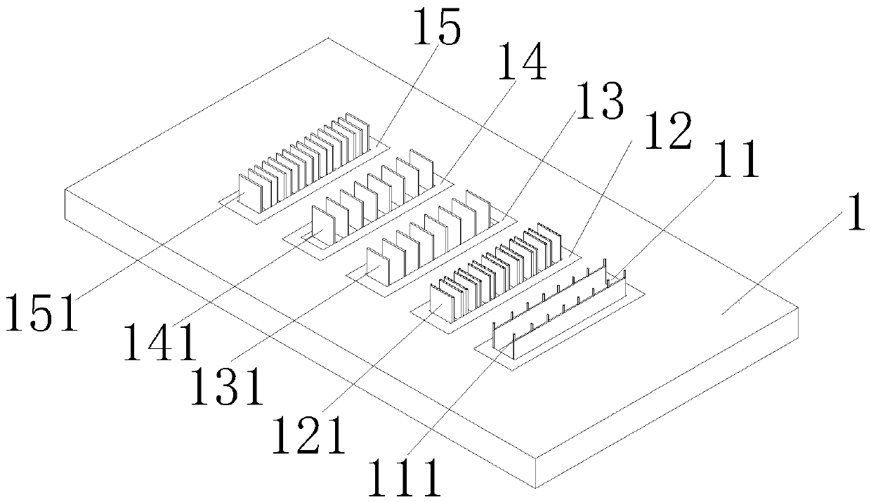
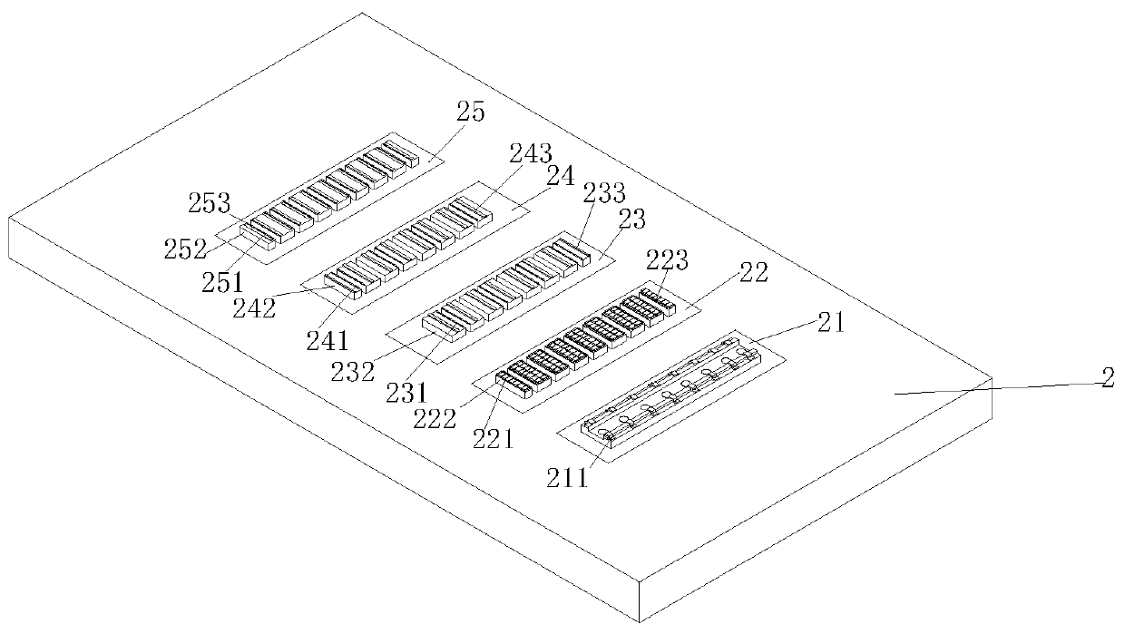
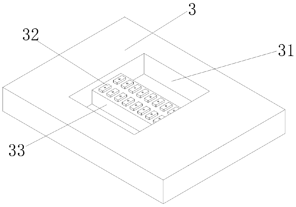
The invention discloses a trimming and forming die for integrated circuit packaging. The die comprises an upper forming die and a lower forming die which are arranged up and down. The upper forming die comprises an upper forming plate, and comprises a gate punching male die, a trimming male die, a cutting male die and a forming male die which are mounted on the upper forming plate. The lower forming die comprises a lower forming plate, and comprises a gate punching male die, a trimming male die, a cutting male die and a forming male die which are installed on the lower forming plate. Through arranging gate punching dies, trimming dies, cutting dies, and forming dies on the upper and lower plates, semi-finished chip materials are enabled to pass through in sequence; glue injection separation, chip trimming, chip cutting and chip forming of plastic package are completed in sequence; the integrated process of chip trimming and forming is achieved. A separating die is arranged to eject outa formed chip material, so that the formed chip material is obtained. The two sets of cutting dies are arranged, and both adopt an interval cutting mode, and the material sequentially passes throughthe two sets of cutting dies to complete chip cutting.

Description

technical field [0001] The invention relates to the technical field of integrated circuit packaging, in particular to an integrated circuit packaging rib cutting molding die. Background technique [0002] Chip packaging is a shell for installing semiconductor integrated circuit chips. It plays the role of placing, fixing, sealing, protecting the chip and enhancing the electrothermal performance. It is also a bridge between the internal world of the chip and the external circuit-the contacts on the chip are connected to On the pins of the package shell, these pins are connected to other devices through the wires on the printed board. Therefore, the package plays an important role for the CPU and other LSI integrated circuits. With the rapid development of the domestic electronics industry, The scale of integrated circuit packaging production continues to expand, and the packaging technology continues to improve from DIP, SOP, TSOP, TQFP to BGA. In order to complete the cuttin...

Claims


Application Information

Patent Timeline
IPC IPC(8): B26F1/44B29C43/36
CPCB26F1/44B26F2001/4427B29C43/36
Inventor 杨标阮怀其
Owner 安徽国晶微电子有限公司
Learn More