A kind of preparation method of thick-film silicon nitride waveguide
A silicon nitride and waveguide technology, applied in the field of integrated optics, can solve problems such as rough side walls and poor waveguide shapes, and achieve the effects of optimizing waveguide shape and side wall roughness, avoiding unevenness, and ensuring waveguide quality
- Summary
- Abstract
- Description
- Claims
- Application Information
AI Technical Summary
Problems solved by technology
Method used
Image
Examples
preparation example Construction
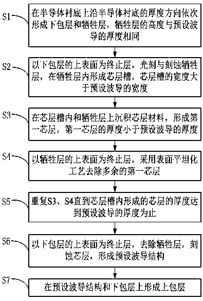
[0026] A method for preparing a thick-film silicon nitride waveguide in this embodiment, such as figure 1 shown, including:
[0027] S1, sequentially forming a lower cladding layer and a sacrificial layer on the semiconductor substrate along the thickness direction of the semiconductor substrate, and the height of the sacrificial layer is the same as the thickness of the preset waveguide;
[0028] On the basis of the above solutions, further, the semiconductor substrate in this implementation manner is a silicon substrate, and in other implementation manners, the semiconductor substrate may also be a quartz substrate.
[0029] On the basis of the above scheme, further, the lower cladding layer is formed by depositing a solid cladding material with a refractive index lower than 1.7 and higher than 1 by thermal oxidation or / and chemical vapor deposition; in other embodiments, the lower cladding layer can also be Formed by physical vapor deposition process. In some embodiments,...
Embodiment 1
[0050] S1, sequentially forming a lower cladding layer and a sacrificial layer on the semiconductor substrate along the thickness direction of the semiconductor substrate, and the height of the sacrificial layer is the same as the thickness of the preset waveguide;
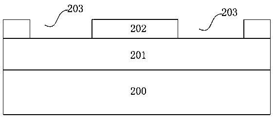
[0051]As shown in FIG. 2 ( 1 ), those skilled in the art can deposit and form the lower cladding layer 201 by thermal oxidation or / and chemical vapor deposition. Wherein, the material of the lower cladding layer 201 can be a solid cladding material with a refractive index lower than 1.7 and higher than 1, silicon dioxide or others, and the material used for the lower cladding layer 201 in this embodiment is preferably silicon dioxide; the sacrificial layer 202 adopts a deposition process, and the material used for the sacrificial layer 202 is preferably amorphous silicon; the material of the semiconductor substrate 200 can be a silicon substrate or a quartz substrate, and the material used for the semiconductor sub...
Embodiment 2
[0067] Compared with embodiment 1, step 1 to step 5 in embodiment 2 are identical with embodiment 1;
[0068] S6. The upper surface of the lower cladding layer is used as a termination layer, the sacrificial layer is removed, and the core layer is etched to form a preset waveguide structure;
[0069] As shown in FIG. 2 ( 11 ), the specific operation is to remove the sacrificial layer 202 by wet etching. Wherein, the process steps of the wet etching are as follows: the wet etching solution is determined according to the ratio of the amorphous silicon in the sacrificial layer 202 to the silicon dioxide in the lower cladding layer 201 . Specifically, a dilute tetramethylammonium hydroxide (TMAH) solution is used for wet etching. The etching rate of the selected wet etching solution to amorphous silicon is greater than that of silicon dioxide and silicon nitride, so that while removing the remaining sacrificial layer 202, no or only a small amount of core Layer 206.
[0070] As...
PUM
| Property | Measurement | Unit |
|---|---|---|
| thickness | aaaaa | aaaaa |
| width | aaaaa | aaaaa |
| width | aaaaa | aaaaa |
Abstract
Description
Claims
Application Information
 - Generate Ideas
- Intellectual Property
- Life Sciences
- Materials
- Tech Scout
- Unparalleled Data Quality
- Higher Quality Content
- 60% Fewer Hallucinations
Browse by: Latest US Patents, China's latest patents, Technical Efficacy Thesaurus, Application Domain, Technology Topic, Popular Technical Reports.
© 2025 PatSnap. All rights reserved.Legal|Privacy policy|Modern Slavery Act Transparency Statement|Sitemap|About US| Contact US: help@patsnap.com


