Implementation method of metal cantilever beam structure

An implementation method and cantilever beam technology are applied in the directions of microstructure technology, microstructure device, manufacturing microstructure device, etc., to achieve the effect of optical anti-shake

Active Publication Date: 2019-10-29
GALAXYCORE SHANGHAI
View PDF4 Cites 0 Cited by
  • Summary
  • Abstract
  • Description
  • Claims
  • Application Information

AI Technical Summary

Problems solved by technology

In the work of semiconductor devices, there are certain functions that need to control and drive semiconductor devices to move in one direction. In the prior art, electromagnetic control or MEMS is often used for control, and the control accuracy needs to be improved. In addition, the existing drive control methods need Larger mechanical devices are inconsistent with the development direction of higher electronic integration requirements. Therefore, how to provide a method for driving objects in the semiconductor field is one of the needs of the industry.

Method used


Image

  • Implementation method of metal cantilever beam structure
  • Implementation method of metal cantilever beam structure
  • Implementation method of metal cantilever beam structure

Examples


Embodiment Construction

[0037] In the following detailed description of the preferred embodiment, reference is made to the accompanying drawings which form a part hereof. The accompanying drawings show, by way of example, specific embodiments in which the invention can be practiced. The illustrated embodiments are not intended to be exhaustive of all embodiments in accordance with the invention. It is to be understood that other embodiments may be utilized and structural or logical changes may be made without departing from the scope of the present invention. Accordingly, the following detailed description is not limiting, and the scope of the invention is defined by the appended claims.

[0038] Specific embodiments of the present invention will be described below in conjunction with the accompanying drawings.

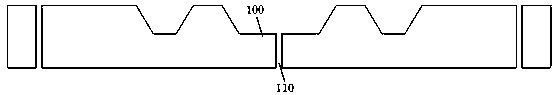
[0039] Please refer to Figure 1 to Figure 10 , Figure 1 to Figure 10 It is a structural diagram corresponding to each step of the metal cantilever implementation method in Embodiment 1...


PUM


Abstract

The invention provides an implementation method of a metal cantilever beam structure. The implementation method comprises the following steps: providing a mold with a concave-convex structure on the surface; electroplating or chemically plating a layer of metal film, or adhering a layer of metal film on the surface of the concave-convex structure of the mold, and forming the metal film on the surface of the concave-convex structure through external force; providing a semiconductor substrate, and forming a metal circuit layer and metal contact points on the front surface of the semiconductor substrate; integrally attaching the mold and a metal film to the front surface of a semiconductor substrate; wherein the metal film is attached to and electrically connected with the metal contact points; removing the mold; and removing partial region of the suspended metal film to form a metal cantilever beam structure.

Description

technical field [0001] The invention relates to the technical field of semiconductors, in particular to a method for realizing a metal cantilever beam. Background technique [0002] Semiconductors are the foundation of modern industry. With the advent of the information and digital age, the penetration rate of electronic products has reached a very high level. As the basic components of electronic products, semiconductors have played a pivotal role. In the work of semiconductor devices, there are certain functions that need to control and drive semiconductor devices to move in one direction. In the prior art, electromagnetic control or MEMS is often used for control, and the control accuracy needs to be improved. In addition, the existing drive control methods need Larger mechanical devices are inconsistent with the development direction of higher electronic integration requirements. Therefore, how to provide a method for driving objects in the semiconductor field is one of ...

Claims


Application Information

Patent Timeline
IPC IPC(8): B81C1/00H01L27/146
CPCB81C1/0015B81C1/00531H01L27/14618
Inventor 赵立新蒋珂玮
Owner GALAXYCORE SHANGHAI
Why Eureka
Try Eureka