Supercharge Your Innovation With Domain-Expert AI Agents!
RF power transistors with impedance matching circuits, and methods of manufacture thereof
What is Al technical title?
Al technical title is built by PatSnap Al team. It summarizes the technical point description of the patent document.
A transistor and circuit technology, applied in the field of packaging semiconductor devices
Active Publication Date: 2019-06-07
NXP USA INC
View PDF18 Cites 1 Cited by
Summary
Abstract
Description
Claims
Application Information
AI Technical Summary
This helps you quickly interpret patents by identifying the three key elements:
Problems solved by technology
Method used
Benefits of technology
Problems solved by technology
More specifically, the inductance of the bond wires interconnecting the various output circuit components can limit the LFR of the device
Method used
Image
Click on the blue label to locate the original text in one second.
Reading with bidirectional positioning of images and text.
Examples
Embodiment Construction
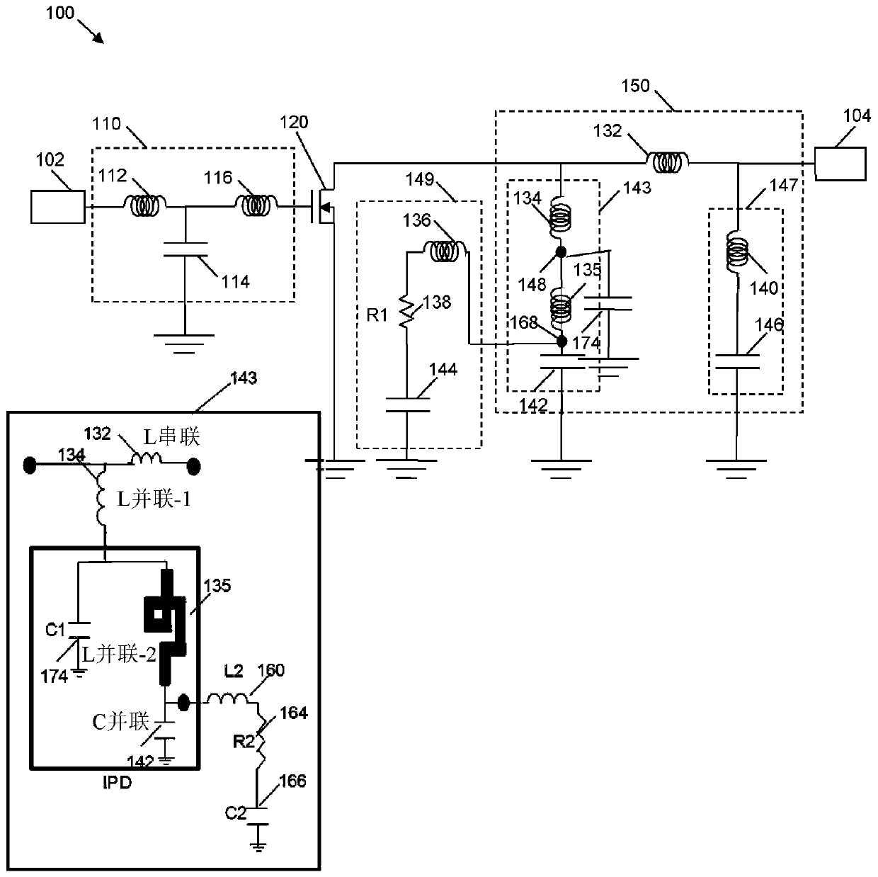
[0050]An output impedance matching circuit in a conventional RF power amplifier device may include a parallel circuit used as a high-pass matching stage, and the like. For example, a conventional parallel circuit may include an inductor (herein a "shunt inductor" or L 并联 ) and capacitors (herein “parallel capacitors” or C 并联 ). In conventional setups, the "RF cold spot" is located between the shunt inductor and shunt capacitor. Essentially, an RF cold spot is a node that can be used as a virtual ground reference voltage for RF electrical signals.
[0051] Gallium Nitride (GaN) based amplifiers have been introduced for cellular macro base stations to improve efficiency and operating bandwidth. GaN transistors offer several advantages as high power final amplifiers compared to silicon based laterally diffused metal oxide semiconductor (Si-LDMOS) transistors. For example, GaN transistors can have 10 times higher power density compared to Si-LDMOS transistors. However, the tr...
PUM
Abstract
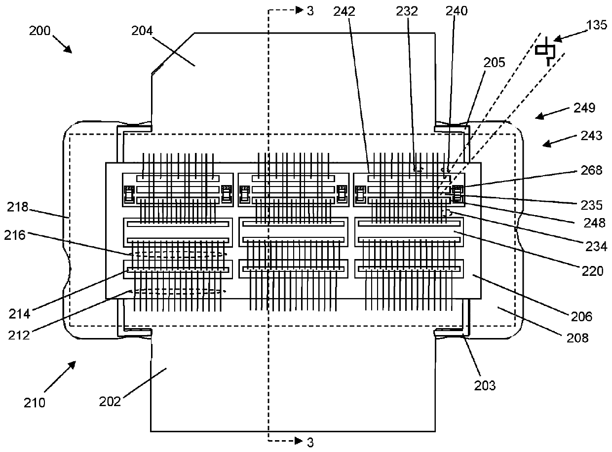
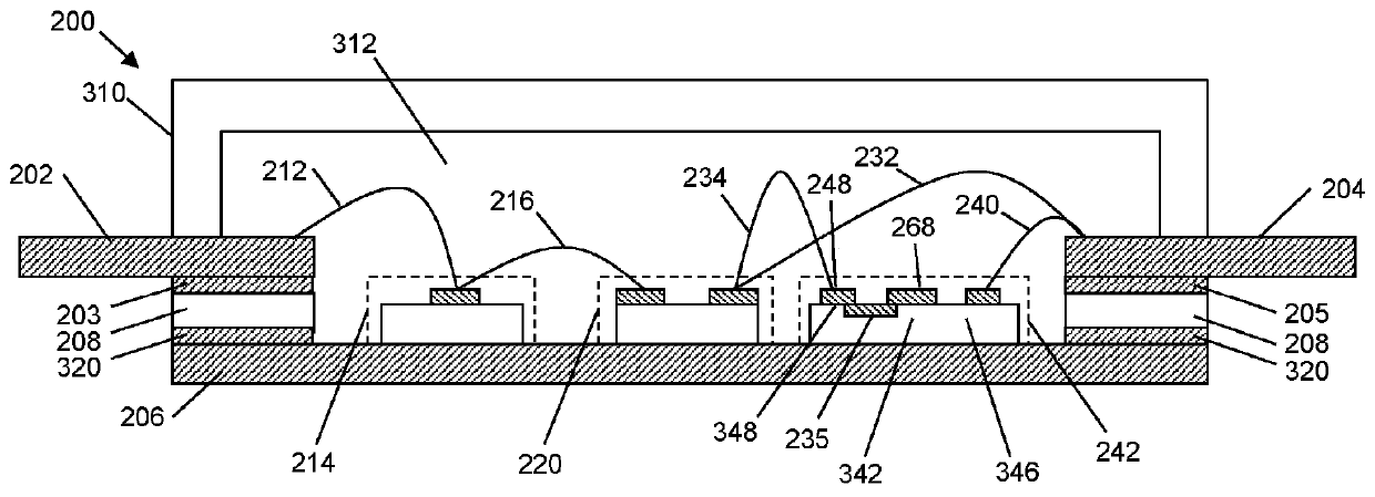
The invention relates to RF power transistors with impedance matching circuits, and methods of manufacture thereof. Embodiments of an RF amplifier include a transistor (120, 220) with a control terminal and first and second current carrying terminals, and a shunt circuit coupled between the first current carrying terminal and a ground reference node. The shunt circuit is an output pre-match impedance conditioning shunt circuit, which includes a first shunt inductance (134, 234, 434), a second shunt inductance (135, 135,235, 435, 935, 935') and a shunt capacitor (142, 142',342, 442) coupled inseries. The first shunt inductance (134, 234, 434) comprises a plurality of bondwires coupled between the first current carrying terminal and the second shunt inductance, and the second shunt inductance (135, 135',235, 435, 935, 935') comprises an integrated inductor coupled between the first shunt inductance and a first terminal of the shunt capacitor (142,142',342, 442). The shunt capacitor is configured to provide capacitive harmonic control of an output of the transistor (120, 220).
Description
technical field [0001] Embodiments of the subject matter described herein relate generally to packaged semiconductor devices, and more particularly to packaged radio frequency (RF) semiconductor devices that include impedance matching circuits. Background technique [0002] A typical high power radio frequency (RF) semiconductor device may include one or more input leads, one or more output leads, one or more transistors, bond wires coupling the input leads to the transistors, and coupling the transistors to the output leads the bonding wire. Bond wires have significant inductance at high frequencies, and this inductance is factored into the design of the device's input and output impedance matching circuits. In some cases, the input and output impedance matching circuits may be contained within the same package that contains the device transistors. More specifically, an in-package input impedance matching circuit may be coupled between the input lead of the device and the...
Claims
Application Information
Patent Timeline
Application Date:The date an application was filed.
Publication Date:The date a patent or application was officially published.
First Publication Date:The earliest publication date of a patent with the same application number.
Issue Date:Publication date of the patent grant document.
PCT Entry Date:The Entry date of PCT National Phase.
Estimated Expiry Date:The statutory expiry date of a patent right according to the Patent Law, and it is the longest term of protection that the patent right can achieve without the termination of the patent right due to other reasons(Term extension factor has been taken into account ).
Invalid Date:Actual expiry date is based on effective date or publication date of legal transaction data of invalid patent.
