Flexible circuit board, capacitive screen and flexible circuit board processing method

A technology of flexible circuit boards and conductive sheets, which is applied to printed circuit components, electrical digital data processing, and electrical connection printed components, etc. It can solve problems such as poor contact of flexible circuit boards, and achieves avoiding poor contact, simple processing, and simplified processing The effect of craft

Active Publication Date: 2020-08-28
GUANGZHOU SHIYUAN ELECTRONICS CO LTD +1
View PDF9 Cites 0 Cited by
  • Summary
  • Abstract
  • Description
  • Claims
  • Application Information

AI Technical Summary

Problems solved by technology

[0004] The purpose of the present invention is to improve the defects of the prior art and provide a flexible circuit board, capacitive screen and flexible circuit board processing method. The conductive connection structure of the present invention is stable and can solve the problem of poor contact of the flexible circuit board

Method used


Image

  • Flexible circuit board, capacitive screen and flexible circuit board processing method
  • Flexible circuit board, capacitive screen and flexible circuit board processing method
  • Flexible circuit board, capacitive screen and flexible circuit board processing method

Examples


Embodiment 1

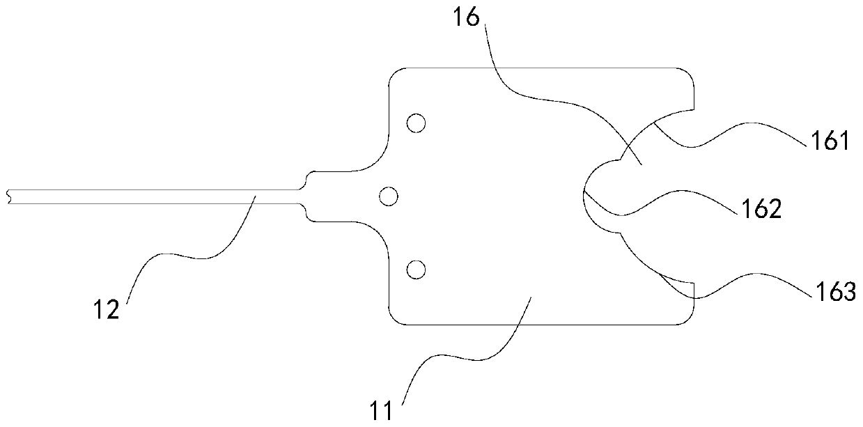
[0064] Such as Figure 1 to Figure 7 As shown, the capacitive screen 50 includes a screen body 51 and a flexible circuit board.

[0065] The flexible circuit board includes: a base layer 22, a conductive layer 10 and a protective layer. The conductive layer 10 is attached to the base layer 22. The protective layer covers the conductive layer 10. The conductive layer 10 has a conductive sheet 11 and a conductive wire 12. The conductive sheet 11 and the conductive wire 12 are electrically connected to each other, the conductive sheet 11 is located at the conductive connection side, and the conductive sheet 11 has a first relief gap 16, and the opening width of the first relief gap 16 gradually decreases from the outside to the inside (this embodiment In an example, the edge of the first abdication 16 is an arc segment).

[0066] There are conductive contacts 52 on the screen body 51, and the back surface of the flexible circuit board is electrically connected to the screen body...

Embodiment 2

[0094] Such as Figure 8 As shown, compared with the first embodiment, this embodiment has the first relief gap 16 whose edge is an arc segment, and there is only one arc segment.

[0095] This embodiment has the following advantages:

[0096] In this embodiment, when processing the conductive sheet 11 , the drill only needs to drill one cut and drill an arc segment to complete the processing of the conductive sheet 11 , and the process of processing the conductive sheet 11 is more convenient.


PUM


Abstract

Disclosed are a flexible circuit board, a capacitance screen (50), and a method for machining the flexible circuit board. The flexible circuit board comprises a base layer (22), and a conductive layer (10), wherein the conductive layer (10) is attached to the base layer (22); the conductive layer (10) is at least provided with a conductive sheet (11) and a conductive wire (12); the conductive sheet (11) and the conductive wire (12) are mutually electrically connected; the conductive sheet (11) is located at a conductive connection side, and a first avoidance notch (16) is provided on the conductive sheet (11); and the opening width of the first avoidance notch (16) gradually reduces from the outside to the inside. The conductive connection structure is stable; the problems of poor contact and binding an open circuit in the flexible circuit board can be solved; process flow time for machining the conductive sheet is short; and a drilling operation is easily carried out, and the structure is more stable and reliable.

Description

technical field [0001] The invention relates to the technical field of capacitive touch screens, in particular to a flexible circuit board, a capacitive screen and a processing method for the flexible circuit board. Background technique [0002] In recent years, since the capacitive touch screen can directly affect the electric field based on the human body, the application of capacitive touch technology in electronic products has become more and more extensive. According to the market and future development direction, the size of the capacitive screen in electronic products has been increasing. [0003] Due to the narrow slot gap of the conductive sheet in the traditional process, the binding strength of the silver glue on the gap is not enough. When the flexible circuit board is bent, the silver glue is prone to cracking and falling off, resulting in poor contact. Contents of the invention [0004] The purpose of the present invention is to improve the defects of the pri...

Claims


Application Information

Patent Timeline
Patent Type & Authority Patents(China)
IPC IPC(8): H05K1/11H05K3/40G06F3/044
CPCG06F3/044H05K1/11H05K3/40
Inventor 马正
Owner GUANGZHOU SHIYUAN ELECTRONICS CO LTD
Why Eureka
Try Eureka