
SOI substrate OLED micro-display device having reflective isolation layer

A technology for microdisplay devices and isolation layers, which is applied in the manufacture of electric solid-state devices, semiconductor devices, and semiconductor/solid-state devices, etc., can solve the problems of pixel cross-color and small device size, and achieves reduction of cross-color, lower product cost, and improved Display quality effects

Pending Publication Date: 2019-05-14
CHINA JILIANG UNIV
View PDF4 Cites 0 Cited by
  • Summary
  • Abstract
  • Description
  • Claims
  • Application Information

AI Technical Summary

Problems solved by technology

However, the device size of microdisplay devices is very small, so extremely high pixel resolution is required, and the interval between pixels is limited to less than one micron, so it is easy to cause cross-color between pixels. Adding a reflective isolation layer between them improves the reality quality of microdisplay devices

Method used


Image

  • SOI substrate OLED micro-display device having reflective isolation layer

Examples


Embodiment Construction

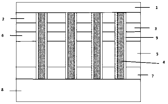
[0010] Describe in detail below in conjunction with the structure of the present invention: figure 1 Among them, an SOI-based OLED microdisplay device with a reflective isolation layer, including a cover glass (1), a color photoresist (2), an encapsulation film layer (3), a transparent cathode (6), and an OLED light-emitting layer (5 ), pixel anode (7), reflective isolation layer (4), SOI substrate (8), silicon dioxide oxide layer (9). It is characterized in that the reflective isolation layer (4) is grown in the gap between the pixel anodes (7) by using Cu metal by electroplating, and the reflective isolation layer (4) is wrapped by a layer of silicon dioxide oxide layer (9). Its manufacturing method Include the following steps:

[0011] 1. Fabricate the pixel anode (7) on the SOI substrate;

[0012] 2. A Cu reflective isolation layer (4) with a thickness of 200nm is electroplated and grown by Damascus process at the interval of the pixel anode (7);

[0013] 3. A silicon d...


PUM


Abstract

The invention provides an SOI substrate OLED micro-display device having a reflective isolation layer, which is relatively high in display quality, small in product volume and wide in application scene. The SOI substrate OLED micro-display device having the reflective isolation layer comprises a glass cover sheet, a colour photoresist, an encapsulation film layer, a transparent cathode, an OLED light emitting layer, a pixel anode, a reflective isolation layer, an SOI substrate and a silicon dioxide oxidization layer. The reflective isolation layer grows in the gap of the pixel anode by adoption of Cu metal through an electroplating method; and the reflective isolation layer is wrapped by the silicon dioxide oxidization layer.

Description

technical field [0001] The invention relates to the field of OLED microdisplay devices, in particular to an SOI substrate OLED microdisplay device with a reflective isolation layer. Background technique [0002] At present, almost all OLED microdisplay device substrates use bulk silicon materials. Compared with bulk silicon, SOI substrates have better isolation. Therefore, applying SOI technology to OLED microdisplays can improve the isolation and at the same time, It can also reduce power consumption and reduce processes. At the same time, the colorization of OLED microdisplay devices on the market today is basically achieved by adding white light and color photoresist. The white light emitted by the pixel anode passes through the RGB color photoresist to emit red, green and blue light. . However, the device size of microdisplay devices is very small, so extremely high pixel resolution is required, and the interval between pixels is limited to less than one micron, so it ...

Claims


Application Information

Patent Timeline
Patent Type & Authority Applications(China)
IPC IPC(8): H01L27/32H01L51/00H01L51/52H01L51/56H10K99/00
Inventor 唐莹杨媚刘祖刚韦一赵红王玉龙柏沁园
Owner CHINA JILIANG UNIV
Learn More